
1SG280LN3F43E3VGS3
| Part Description |
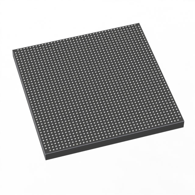
Stratix® 10 GX Field Programmable Gate Array (FPGA) IC 688 2800000 1760-BBGA, FCBGA |
|---|---|
| Quantity | 721 Available (as of June 14, 2026) |

| Product Category | Field Programmable Gate Array (FPGA) |
|---|---|
| Manufacturer | Intel |
| Manufacturing Status | Active |
| Manufacturer Standard Lead Time | 9 Weeks |
| Datasheet |
Specifications & Environmental
| Device Package | 1760-FBGA (42.5x42.5) | Grade | Extended | Operating Temperature | 0°C – 100°C | ||
|---|---|---|---|---|---|---|---|
| Package / Case | 1760-BBGA, FCBGA | Number of I/O | 688 | Voltage | 770 mV - 970 mV | ||
| Mounting Method | Surface Mount | RoHS Compliance | Unknown | REACH Compliance | REACH Unaffected | ||
| Moisture Sensitivity Level | 3 (168 Hours) | Number of LABs/CLBs | 350000 | Number of Logic Elements/Cells | 2800000 | ||
| Number of Gates | N/A | ECCN | N/A | HTS Code | N/A | ||
| Qualification | N/A | Total RAM Bits | 240123904 |
Overview of 1SG280LN3F43E3VGS3 – Stratix® 10 GX FPGA, 2,800,000 logic elements, 688 I/O, 1760-BBGA
The 1SG280LN3F43E3VGS3 is an Intel Stratix® 10 GX field programmable gate array (FPGA) supplied in a 1760‑BBGA / 1760‑FBGA package. It integrates a high-density programmable fabric with a large on-chip memory footprint and extensive I/O to address high-performance compute and high-bandwidth interface applications.
Built on the Stratix® 10 GX family architecture, this device targets designs that require large FPGA capacity and high I/O bandwidth while offering extended-grade temperature operation and a low-voltage core supply range for modern power-optimized systems.
Key Features
- Logic Capacity 2,800,000 logic elements provide a very large programmable fabric for complex algorithms, system aggregation, and wide parallelism.
- On‑Chip Memory 240,123,904 total RAM bits support substantial embedded buffering, streaming data handling, and deep on-chip storage for high-throughput designs.
- I/O Density 688 I/O pins give flexible connectivity for multi-lane transceivers, high-speed interfaces, and broad peripheral support at the package boundary.
- Family Innovations As part of the Stratix® 10 GX family, the device benefits from the Intel Hyperflex core architecture and Intel 14 nm tri-gate process innovations described for the series, enabling higher core performance and power efficiency relative to prior generations.
- High‑Speed Interface Support (Family) Stratix® 10 GX family documentation specifies heterogeneous transceiver tiles and transceiver data rates up to 28.3 Gbps, as well as hard IP such as PCI Express Gen3 and 10G Ethernet options available within the family.
- Power and Supply Core voltage operation from 770 mV to 970 mV enables integration into low-voltage power domains and modern power-optimized system architectures.
- Package and Mounting 1760‑BBGA package case with supplier device package 1760‑FBGA (42.5×42.5) in a surface-mount form factor simplifies board-level integration for compact, high-density PCBs.
- Operating Range and Grade Extended grade device with an operating temperature range from 0 °C to 100 °C suitable for many commercial and mission-critical applications that require wider temperature tolerance.
- Compliance RoHS compliant to meet environmental regulatory requirements for lead-free manufacturing.
Typical Applications
- High‑Performance Networking Large logic capacity and extensive I/O make this device suitable for packet processing, switch/router line cards, and multi‑lane optical/electrical interface functions.
- Data Center Acceleration Substantial on-chip RAM and massive parallel logic resources help implement custom acceleration engines, protocol offloads, and inline processing tasks.
- Telecommunications Infrastructure High I/O count and family transceiver capabilities support backplane and module-level interfaces used in telecom switching and transport equipment.
- Digital Signal Processing Large programmable fabric and memory enable high-throughput DSP algorithms, wideband filters, and multichannel signal chains.
Unique Advantages
- Extremely Large FPGA Fabric: 2,800,000 logic elements allow consolidation of multiple functions or migration of large system-on-FPGA designs into a single device.
- Significant On‑Chip Memory: 240,123,904 bits of RAM support deep buffering and reduce external memory dependency for many high-throughput tasks.
- High I/O Count: 688 I/O pins provide flexible interfacing options for multi-lane links and dense peripheral connectivity without immediate need for multiplexing.
- Family‑Level High‑Speed Capabilities: Stratix® 10 GX family features such as Hyperflex core architecture and high-speed transceivers enable designs that require higher core performance and advanced link performance.
- Compact System Integration: 1760‑BBGA / 1760‑FBGA packaging in a surface-mount form factor supports high-density PCB designs and simplifies mechanical integration.
- Extended‑Grade Operation: 0 °C to 100 °C operating range and extended grade classification provide a broader deployment envelope compared to standard commercial parts.
Why Choose 1SG280LN3F43E3VGS3?
This Stratix® 10 GX device combines very high logic density, large embedded memory, and extensive I/O in a single surface-mount 1760‑BBGA/FBGA package, addressing systems that demand consolidated processing and high-bandwidth interfacing. The device leverages Stratix® 10 family architectural improvements to deliver higher core performance and family-level high-speed interface capabilities for demanding compute and networking applications.
Choose 1SG280LN3F43E3VGS3 for designs that require a high-capacity FPGA with substantial on‑chip RAM and dense I/O, paired with extended-grade operation and RoHS compliance for modern production environments.
Request a quote or submit a pricing inquiry to evaluate 1SG280LN3F43E3VGS3 for your next high-performance FPGA design.


Date Founded: 1968
Headquarters: Santa Clara, California, USA
Employees: 130,000+
Revenue: $54.23 Billion
Certifications and Memberships: ISO9001:2015, ISO14001:2015, ISO17025:2017, ISO27001:2022, ISO45001:2018, ISO50001:2018


