
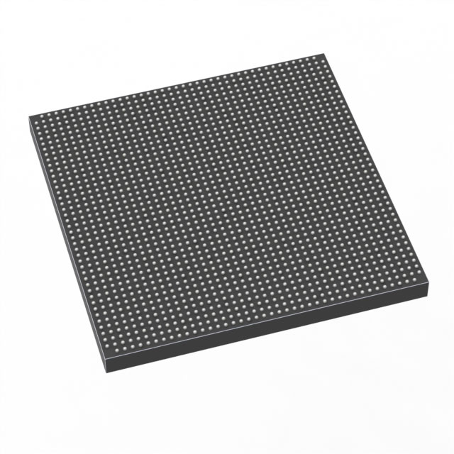
1SG280LU3F50E2VGS3
| Part Description |
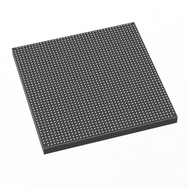
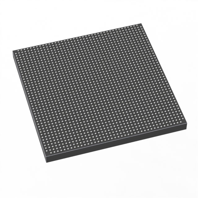
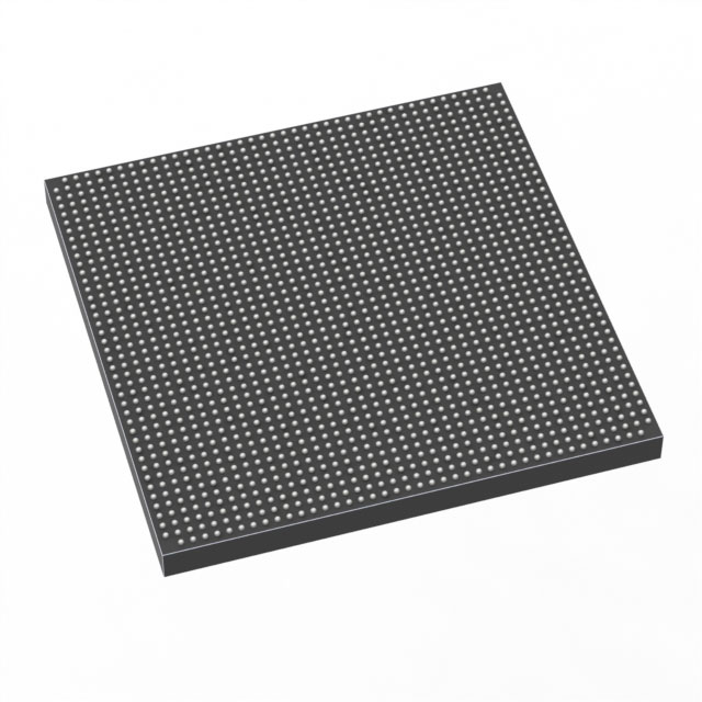
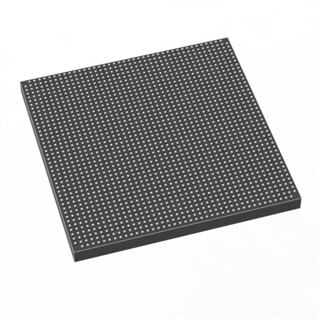
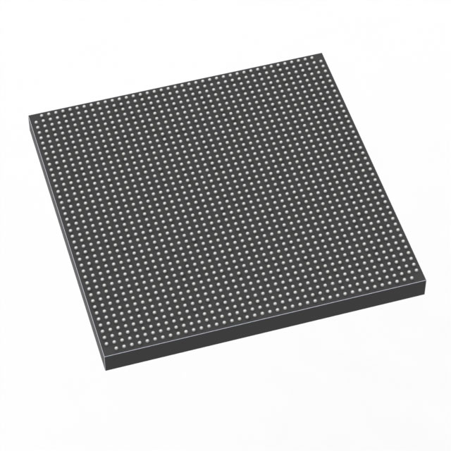
Stratix® 10 GX Field Programmable Gate Array (FPGA) IC 704 2800000 2397-BBGA, FCBGA |
|---|---|
| Quantity | 406 Available (as of October 8, 2026) |
| Product Category | Field Programmable Gate Array (FPGA) |
|---|---|
| Manufacturer | Intel |
| Manufacturing Status | Discontinued |
| Manufacturer Standard Lead Time | 9 Weeks |
| Datasheet |
Specifications & Environmental
| Device Package | 2397-FBGA, FC (50x50) | Grade | Extended | Operating Temperature | 0°C – 100°C | ||
|---|---|---|---|---|---|---|---|
| Package / Case | 2397-BBGA, FCBGA | Number of I/O | 704 | Voltage | 770 mV - 970 mV | ||
| Mounting Method | Surface Mount | RoHS Compliance | Unknown | REACH Compliance | REACH Unaffected | ||
| Moisture Sensitivity Level | 3 (168 Hours) | Number of LABs/CLBs | 350000 | Number of Logic Elements/Cells | 2800000 | ||
| Number of Gates | N/A | ECCN | N/A | HTS Code | N/A | ||
| Qualification | N/A | Total RAM Bits | 240123904 |
Overview of 1SG280LU3F50E2VGS3 – Stratix® 10 GX FPGA, 2,800,000 logic elements, 704 I/Os, 2397‑BBGA
The 1SG280LU3F50E2VGS3 is a Stratix® 10 GX field programmable gate array (FPGA) IC designed for high‑performance, bandwidth‑intensive applications. Built on the Stratix 10 family innovations, it combines the Intel Hyperflex™ core architecture and Intel 14 nm tri‑gate (FinFET) process technology to address demanding processing and connectivity requirements.
This device provides a large logic fabric, extensive on‑chip memory, and high‑speed I/O capability in a 2397‑BBGA (FCBGA) package, making it suitable for advanced networking, communications, compute acceleration, and high‑density FPGA implementations that require significant logic, memory, and I/O resources.
Key Features
- Core Architecture: Intel Hyperflex™ core architecture delivering improved core performance compared to previous generation high‑performance FPGAs as described for the Stratix 10 family.
- Process Technology: Built with Intel 14 nm tri‑gate (FinFET) technology as described in the Stratix 10 device family documentation.
- Logic Capacity: 2,800,000 logic elements (cells) provide extensive programmable fabric for complex designs and high gate counts.
- On‑Chip Memory: 240,123,904 total RAM bits of internal SRAM to support large buffering, caches, and memory‑intensive logic functions.
- High‑Speed I/O and Transceivers: 704 general‑purpose I/Os and family‑level transceiver capabilities (family documentation cites transceiver data rates up to 28.3 Gbps and advanced transceiver features) for high‑bandwidth serial links and backplane interfaces.
- Connectivity IP: Stratix 10 family documentation lists hard IP such as PCI Express Gen3 x16 and 10G/40G Ethernet FEC implemented in transceiver channels; suitable for designs requiring integrated protocol IP (family feature).
- Power Supply Range: Core voltage supply 770 mV to 970 mV, enabling integration into low‑voltage power domains.
- Package & Mounting: 2397‑BBGA (FCBGA) supplier device package 2397‑FBGA, FC (50×50) in a surface‑mount form factor for high‑density board integration.
- Operating Range & Grade: Extended grade with operating temperature range 0 °C to 100 °C and RoHS compliance for regulatory and environmental standards.
Typical Applications
- High‑Performance Networking & Switching: Large logic capacity and high‑speed transceiver capability support packet processing, line cards, and switch fabric implementations that require deep, programmable logic and fast serial I/O.
- Data Center Acceleration & NICs: On‑chip memory and family‑level PCI Express hard IP make the device suitable for NICs, smartNICs, and accelerator cards where low‑latency data movement and protocol offload are required.
- Telecom & Backplane Communications: High transceiver data‑rate capability and large I/O counts enable backplane links, forward error correction, and high‑speed serial protocols for telecom equipment.
- DSP and Compute Offload: Large logic fabric and substantial on‑chip memory support complex DSP pipelines, variable‑precision compute, and algorithm acceleration that need abundant resources and memory bandwidth.
Unique Advantages
- High Logic Density: 2,800,000 logic elements allow implementation of large, complex custom logic, reducing the need for multiple devices in space‑constrained designs.
- Substantial On‑Chip Memory: 240,123,904 RAM bits support large buffers and state storage directly on the FPGA fabric, improving system latency and throughput.
- Advanced I/O and SerDes Capability: 704 I/Os paired with family‑level high‑speed transceiver features enable wide parallel interfaces and high‑bandwidth serial links for modern communications systems.
- Low‑Voltage Core Operation: 770 mV to 970 mV core voltage range aligns with modern power architectures and helps system designers manage power delivery on high‑density boards.
- Footprint for High‑Density Boards: 2397‑BBGA (50×50 FCBGA) package and surface‑mount mounting support compact board layouts while providing extensive I/O and thermal mass.
- Extended Temperature Grade: Rated for 0 °C to 100 °C operation to match a broad class of commercial and extended‑environment systems.
Why Choose 1SG280LU3F50E2VGS3?
This Stratix® 10 GX device delivers a combination of large logic capacity, abundant on‑chip memory, and extensive I/O in a high‑density FCBGA package—making it well suited for advanced networking, compute acceleration, and communication systems that demand programmable performance and high bandwidth. Family innovations such as the Hyperflex core architecture and 14 nm tri‑gate process provide documented gains in core performance and power characteristics for Stratix 10 devices.
Designers and system architects requiring scalable logic resources, robust memory, and high‑speed interfaces will find the 1SG280LU3F50E2VGS3 appropriate for complex, high‑throughput applications where integration and I/O bandwidth are primary design drivers. RoHS compliance and the extended operating grade support deployment across a range of commercial and extended‑environment projects.
Request a quote or submit an inquiry for pricing and availability of the 1SG280LU3F50E2VGS3 to evaluate this FPGA for your next high‑performance design.





















Date Founded: 1968
Headquarters: Santa Clara, California, USA
Employees: 130,000+
Revenue: $54.23 Billion
Certifications and Memberships: ISO9001:2015, ISO14001:2015, ISO17025:2017, ISO27001:2022, ISO45001:2018, ISO50001:2018


