
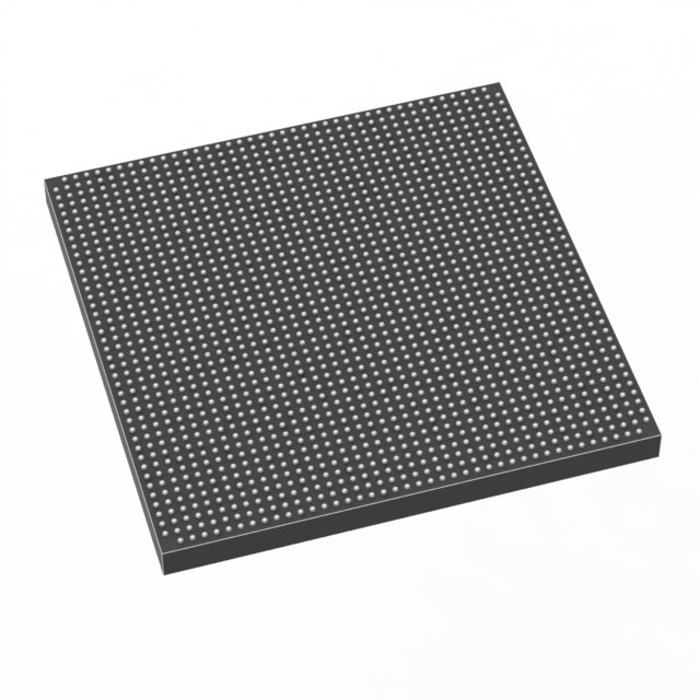
1SG280LU3F50I2VGAS
| Part Description |
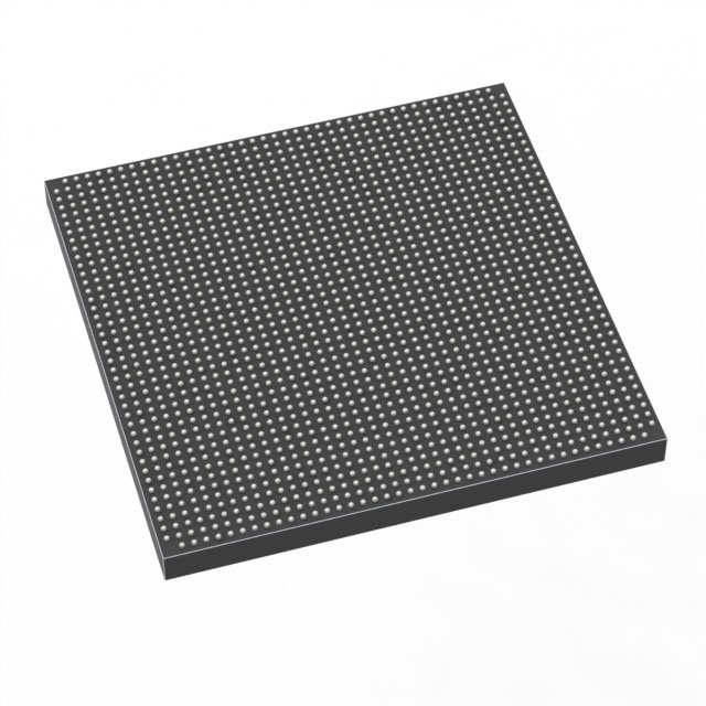
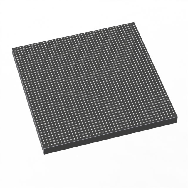
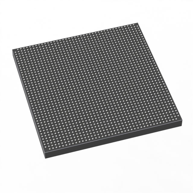
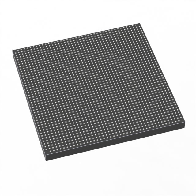
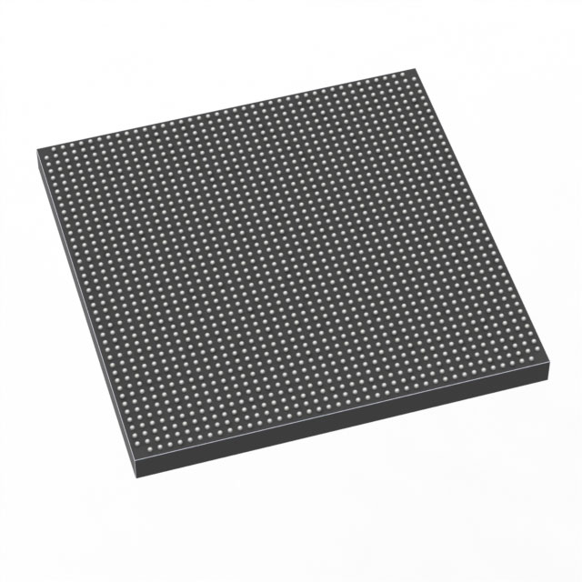
Stratix® 10 GX Field Programmable Gate Array (FPGA) IC 704 2800000 2397-BBGA, FCBGA |
|---|---|
| Quantity | 1,213 Available (as of October 7, 2026) |
| Product Category | Field Programmable Gate Array (FPGA) |
|---|---|
| Manufacturer | Intel |
| Manufacturing Status | Active |
| Manufacturer Standard Lead Time | 12 Weeks |
| Datasheet |
Specifications & Environmental
| Device Package | 2397-FBGA, FC (50x50) | Grade | Industrial | Operating Temperature | -40°C – 100°C | ||
|---|---|---|---|---|---|---|---|
| Package / Case | 2397-BBGA, FCBGA | Number of I/O | 704 | Voltage | 770 mV - 970 mV | ||
| Mounting Method | Surface Mount | RoHS Compliance | Unknown | REACH Compliance | REACH Unaffected | ||
| Moisture Sensitivity Level | 3 (168 Hours) | Number of LABs/CLBs | 350000 | Number of Logic Elements/Cells | 2800000 | ||
| Number of Gates | N/A | ECCN | N/A | HTS Code | N/A | ||
| Qualification | N/A | Total RAM Bits | 240123904 |
Overview of 1SG280LU3F50I2VGAS – Stratix® 10 GX Field Programmable Gate Array (FPGA) IC 704 2800000 2397-BBGA, FCBGA
The 1SG280LU3F50I2VGAS is an Intel Stratix® 10 GX FPGA optimized for high-bandwidth, processing‑intensive designs. As part of the Stratix 10 GX family, the device leverages the Intel Hyperflex™ core architecture and Intel 14 nm tri‑gate (FinFET) technology to address demanding FPGA applications.
This industrial‑grade, surface‑mount FPGA provides a combination of large logic capacity, extensive on‑chip RAM and high I/O/transceiver density for systems that require scalable programmable logic, advanced interface support and robust configuration and security capabilities.
Key Features
- Core & Architecture Built on the Intel Hyperflex core architecture and 14 nm tri‑gate (FinFET) process for improved core performance and power efficiency across the Stratix 10 GX family.
- Logic Capacity Approximately 2,800,000 logic elements and 350,000 logic blocks to implement large, complex hardware designs and partitioned functions.
- On‑Chip Memory 240,123,904 total RAM bits of embedded memory for buffering, packet processing, and deep pipeline storage requirements.
- I/O and Transceiver Capability 704 general‑purpose I/Os and family‑level high‑speed serial transceiver capabilities (family transceiver performance up to 28.3 Gbps and multi‑channel support) for high‑bandwidth interfaces and packet I/O.
- Hard IP and DSP Family features include hard PCI Express Gen3, 10G Ethernet and high‑efficiency variable precision DSP blocks to accelerate common protocol and signal‑processing tasks.
- Power and Voltage Core supply operating range of 770 mV to 970 mV to support low‑voltage operation and power management strategies.
- Package & Mounting Surface‑mount package in 2397‑BBGA, FCBGA format (supplier package: 2397‑FBGA, FC (50x50)) for high‑density board integration.
- Industrial Temperature Range Rated for operation from −40 °C to 100 °C for deployment in industrial environments.
- Configuration, Security & Reliability Family documentation details secure device management, partial and dynamic reconfiguration capabilities, and SEU error detection and correction features to support resilient, field‑upgradable systems.
- Regulatory RoHS compliant.
Typical Applications
- High‑Performance Networking & Switching Use the device’s large logic and on‑chip RAM to implement packet processing, traffic management and line‑rate switching functions.
- Telecommunications & Optical Transport High‑speed transceiver capability and protocol hard IP make the device suitable for backplane and module interfaces in telecom systems.
- Data Center Acceleration Implement custom accelerators and protocol offloads where large programmable logic capacity and DSP resources reduce latency and increase throughput.
- Test, Measurement & Instrumentation Combine high I/O density and embedded memory to handle wideband data capture, preprocessing and interfacing for measurement systems.
Unique Advantages
- Massive Logic Scale: 2.8 million logic elements enable integration of multiple complex subsystems on a single device, reducing BOM and interconnect complexity.
- Significant On‑Chip Memory: 240+ million RAM bits provide headroom for deep buffering, lookup tables and large state machines without external memory.
- High I/O and High‑Speed Links: 704 I/Os combined with family transceiver performance support dense front‑end connectivity and multi‑lane, multi‑protocol interfaces.
- Industrial Temperature Rating: −40 °C to 100 °C operation supports reliable deployment in industrial and ruggedized systems.
- Secure, Flexible Configuration: Family features for secure device management, partial/dynamic reconfiguration and SEU mitigation simplify field updates and enhance system uptime.
- Package Density: 2397‑BBGA/FCBGA package (50x50) enables compact board area for high‑density system designs.
Why Choose 1SG280LU3F50I2VGAS?
The 1SG280LU3F50I2VGAS delivers the performance and integration expected from the Stratix 10 GX family: a large logic fabric, abundant embedded memory, extensive I/O and high‑speed serial capability, all in an industrial‑rated, surface‑mount package. It is suited for engineering teams building high‑bandwidth, compute‑intensive and interface‑dense systems where consolidation of functions into a single FPGA reduces board complexity and accelerates time to market.
Supported by Stratix 10 family architecture and configuration/security features, this device provides long‑term value for scalable designs that require robust programmability, hardware acceleration and dependable operation across industrial temperature ranges.
Request a quote or submit an inquiry to receive pricing and availability information for 1SG280LU3F50I2VGAS.





















Date Founded: 1968
Headquarters: Santa Clara, California, USA
Employees: 130,000+
Revenue: $54.23 Billion
Certifications and Memberships: ISO9001:2015, ISO14001:2015, ISO17025:2017, ISO27001:2022, ISO45001:2018, ISO50001:2018


