
1ST040EH1F35I2VG
| Part Description |
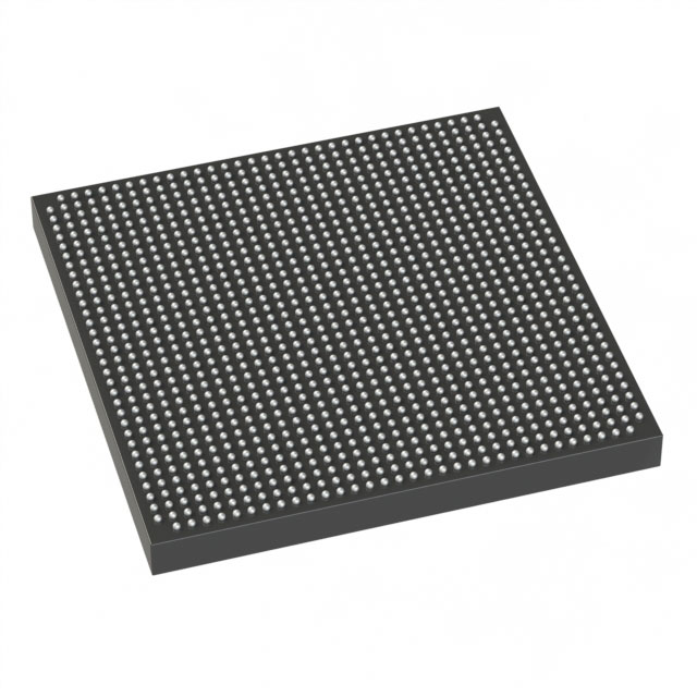
Stratix® 10 TX Field Programmable Gate Array (FPGA) IC 384 31457280 378000 1152-BBGA, FCBGA |
|---|---|
| Quantity | 138 Available (as of June 16, 2026) |

| Product Category | Field Programmable Gate Array (FPGA) |
|---|---|
| Manufacturer | Intel |
| Manufacturing Status | Active |
| Manufacturer Standard Lead Time | 12 Weeks |
| Datasheet |
Specifications & Environmental
| Device Package | 1152-FBGA (35x35) | Grade | Industrial | Operating Temperature | -40°C – 100°C | ||
|---|---|---|---|---|---|---|---|
| Package / Case | 1152-BBGA, FCBGA | Number of I/O | 384 | Voltage | 770 mV - 970 mV | ||
| Mounting Method | Surface Mount | RoHS Compliance | Unknown | REACH Compliance | REACH Unknown | ||
| Moisture Sensitivity Level | 3 (168 Hours) | Number of LABs/CLBs | N/A | Number of Logic Elements/Cells | 378000 | ||
| Number of Gates | N/A | ECCN | N/A | HTS Code | N/A | ||
| Qualification | N/A | Total RAM Bits | 31457280 |
Overview of 1ST040EH1F35I2VG – Stratix® 10 TX FPGA, 378000 logic elements, 31,457,280-bit RAM, 384 I/O
The 1ST040EH1F35I2VG is a Stratix® 10 TX field programmable gate array (FPGA) from Intel, offering high-density programmable logic with 378,000 logic elements and 31,457,280 total RAM bits. This industrial-grade, surface-mount device provides 384 I/O and operates across a 770 mV to 970 mV supply range.
Packaged in a 1152-FBGA (35×35) / 1152-BBGA FCBGA form factor and rated for −40 °C to 100 °C, the device targets systems that require large on-chip memory, extensive logic resources, and robust I/O capability within an industrial temperature envelope.
Key Features
- Core Logic 378,000 logic elements provide substantial programmable logic capacity for complex custom architectures and parallel compute tasks.
- On-Chip Memory 31,457,280 total RAM bits enable large buffering, state storage, and data-path implementations without immediate external memory dependence.
- I/O Resources 384 I/O pins support wide peripheral interfacing and multi-channel connectivity for mixed-signal and multi-protocol systems.
- Power Supply Operates from 770 mV to 970 mV supply rails, enabling designs that target specific core-voltage domains.
- Package & Mounting Available in a 1152-FBGA (35×35) supplier package and listed as 1152-BBGA, FCBGA; intended for surface-mount PCB assembly.
- Temperature & Grade Industrial grade with an operating temperature range of −40 °C to 100 °C for deployment in temperature-challenging environments.
- Environmental Compliance RoHS compliant.
Typical Applications
- Industrial Control Leverages the device’s high logic density and on-chip RAM to implement custom control algorithms, I/O aggregation, and real-time data handling in industrial systems.
- Signal Processing Large RAM and extensive logic elements support implementation of buffering, filtering, and custom datapaths for high-throughput signal processing tasks.
- Communications & Networking Broad I/O and sizable programmable resources enable protocol aggregation, packet processing, and interface bridging in infrastructure equipment.
- Test & Measurement Flexible logic and on-chip memory support custom measurement sequencing, data capture, and preprocessing functions in instrumentation designs.
Unique Advantages
- High logic capacity: 378,000 logic elements give designers room to implement complex algorithms and parallel processing pipelines on a single device.
- Substantial on-chip RAM: 31,457,280 total RAM bits reduce reliance on external memory for many buffering and state-storage needs, simplifying BOM and layout.
- Extensive I/O: 384 I/O pins enable broad peripheral connectivity and multi-channel interfacing without additional bridge devices.
- Industrial temperature rating: −40 °C to 100 °C operating range allows deployment in temperature-challenging environments typical of industrial applications.
- Compact board-level integration: 1152-FBGA (35×35) / 1152-BBGA package supports high-density PCB integration while keeping the device surface-mount compatible.
- Regulatory readiness: RoHS compliance simplifies environmental conformity for global product designs.
Why Choose 1ST040EH1F35I2VG?
The 1ST040EH1F35I2VG combines abundant programmable logic, large on-chip memory, and broad I/O in an industrial-grade FPGA package, making it suitable for designs that demand integrated compute and interface capability within a compact surface-mount form factor. Its operating voltage and temperature specifications enable designers to plan power domains and thermal profiles with clear, verifiable limits.
This device is well suited for engineers building industrial control systems, signal processing accelerators, communications infrastructure, and test equipment that require significant on-chip resources and robust environmental performance.
Request a quote or submit an inquiry today to evaluate 1ST040EH1F35I2VG for your next design.


Date Founded: 1968
Headquarters: Santa Clara, California, USA
Employees: 130,000+
Revenue: $54.23 Billion
Certifications and Memberships: ISO9001:2015, ISO14001:2015, ISO17025:2017, ISO27001:2022, ISO45001:2018, ISO50001:2018


