
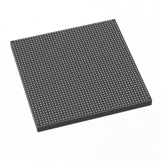
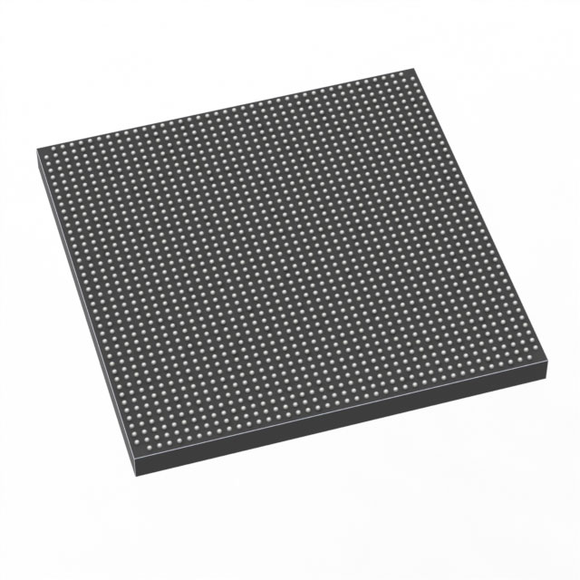
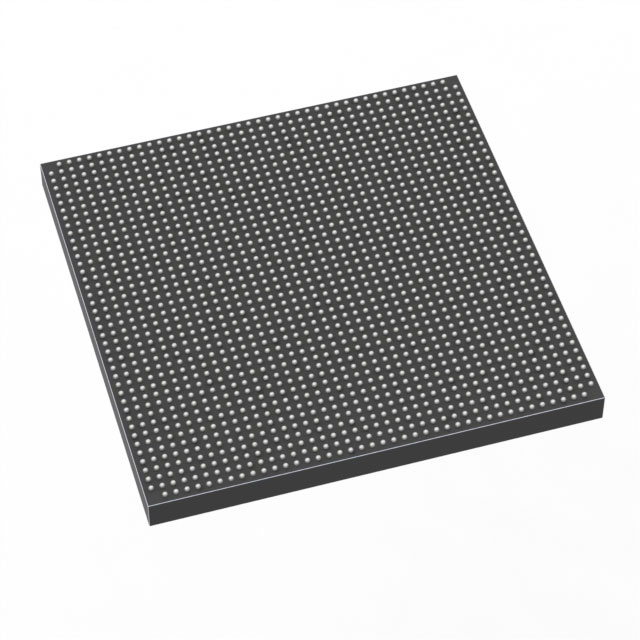
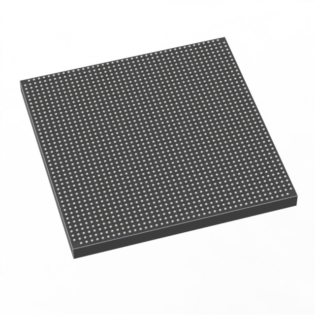
1ST110ES3F50E3VG
| Part Description |
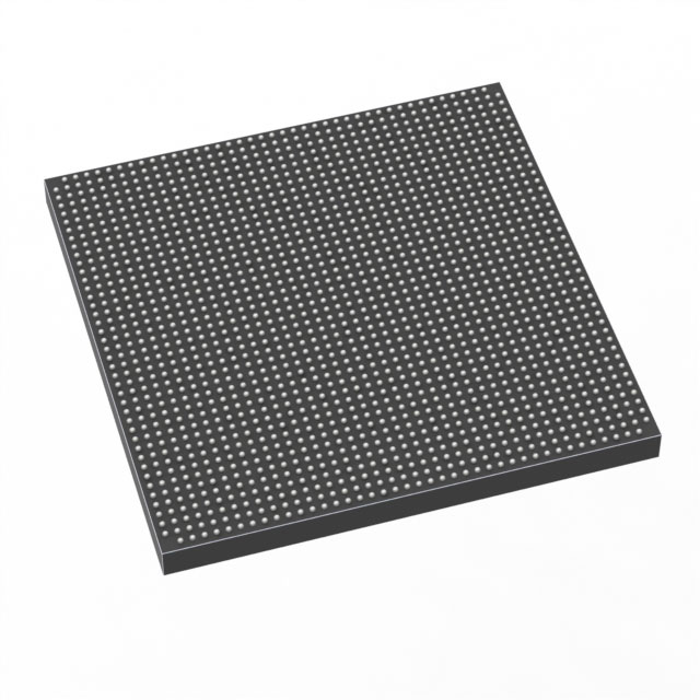
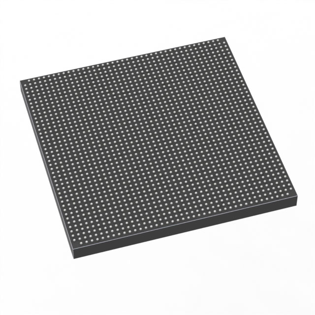
Stratix® 10 TX Field Programmable Gate Array (FPGA) IC 440 112197632 1325000 2397-BBGA, FCBGA |
|---|---|
| Quantity | 520 Available (as of October 8, 2026) |
| Product Category | Field Programmable Gate Array (FPGA) |
|---|---|
| Manufacturer | Intel |
| Manufacturing Status | Active |
| Manufacturer Standard Lead Time | 12 Weeks |
| Datasheet |
Specifications & Environmental
| Device Package | 2397-FBGA, FC (50x50) | Grade | Extended | Operating Temperature | 0°C – 100°C | ||
|---|---|---|---|---|---|---|---|
| Package / Case | 2397-BBGA, FCBGA | Number of I/O | 440 | Voltage | 770 mV - 970 mV | ||
| Mounting Method | Surface Mount | RoHS Compliance | Unknown | REACH Compliance | REACH Unknown | ||
| Moisture Sensitivity Level | 3 (168 Hours) | Number of LABs/CLBs | N/A | Number of Logic Elements/Cells | 1325000 | ||
| Number of Gates | N/A | ECCN | N/A | HTS Code | N/A | ||
| Qualification | N/A | Total RAM Bits | 112197632 |
Overview of 1ST110ES3F50E3VG – Stratix® 10 TX Field Programmable Gate Array (FPGA) IC 440 112197632 1325000 2397-BBGA, FCBGA
The 1ST110ES3F50E3VG is a Stratix® 10 TX field programmable gate array (FPGA) IC delivering high logic density and substantial on-chip RAM for complex digital designs. Its architecture targets applications that require large numbers of logic elements, extensive embedded memory, and a significant I/O count within a surface-mount FCBGA package.
With 1,325,000 logic elements, 112,197,632 total RAM bits, and 440 I/O pins, this device is positioned to support compute-heavy, memory-intensive, and I/O-rich system designs while operating across a 0 °C to 100 °C range and a core supply window of 770 mV to 970 mV.
Key Features
- Core Logic 1,325,000 logic elements provide high-density programmable fabric for complex algorithms, custom accelerators, and large-scale state machines.
- On-Chip Memory 112,197,632 total RAM bits enable extensive buffering, large lookup tables, and memory-centric processing without external RAM dependency.
- I/O Capacity 440 general-purpose I/O pins support dense board connectivity and multiple parallel interfaces.
- Power Supply Core voltage operating range of 770 mV to 970 mV allows integration into systems with defined low-voltage power rails.
- Package & Mounting 2397-BBGA/FCBGA package (2397-FBGA, FC 50×50) in a surface-mount form factor facilitates high-pin-count integration on compact PCBs.
- Temperature & Grade Extended grade operation from 0 °C to 100 °C for designs needing above-room-temperature capability without industrial-grade claims.
- Compliance RoHS compliant to support environmentally conscious design requirements.
Typical Applications
- High-density digital processing Use the device where large programmable logic capacity is required for custom datapaths, packet processing, or complex control logic.
- Memory-intensive designs Leverage the extensive on-chip RAM for buffering, large lookup tables, and embedded data storage to reduce external memory dependence.
- I/O-rich systems Deploy in applications that need many parallel interfaces or numerous signal connections, supported by 440 I/O pins.
- Custom accelerator integration Implement hardware accelerators and specialized processing blocks that benefit from high logic and memory resources.
Unique Advantages
- High logic capacity: 1,325,000 logic elements enable large, complex FPGA designs without partitioning across multiple devices.
- Substantial on-chip memory: 112,197,632 RAM bits reduce reliance on external memory, improving latency and simplifying BOM.
- Large I/O count: 440 I/O pins simplify board-level connectivity for multi-channel or parallel-interface designs.
- Compact high-pin-count package: 2397-FBGA (50×50) FCBGA package concentrates functionality in a surface-mount form factor suitable for dense PCB layouts.
- Extended temperature grade: Rated 0 °C to 100 °C to support designs operating above ambient temperatures without implying industrial-grade qualification.
- RoHS compliance: Meets environmental compliance expectations for modern electronic assemblies.
Why Choose 1ST110ES3F50E3VG?
The 1ST110ES3F50E3VG combines very high logic element count, a large embedded memory pool, and extensive I/O in a single surface-mount FCBGA package, positioning it for demanding, memory- and logic-heavy designs. Its extended temperature range and RoHS compliance make it suitable for a broad set of commercial and industrial-adjacent applications where higher than room-temperature operation is required.
This device is well suited to engineering teams building compute- or data-intensive systems that benefit from integrated memory and high I/O density, offering a compact physical footprint and a clear specification set for power and thermal planning.
Request a quote or submit your requirements to receive pricing and availability information for the 1ST110ES3F50E3VG. Our team can provide supply details and support for your design evaluation and procurement process.





















Date Founded: 1968
Headquarters: Santa Clara, California, USA
Employees: 130,000+
Revenue: $54.23 Billion
Certifications and Memberships: ISO9001:2015, ISO14001:2015, ISO17025:2017, ISO27001:2022, ISO45001:2018, ISO50001:2018


