
1ST250EU3F50E3XG
| Part Description |
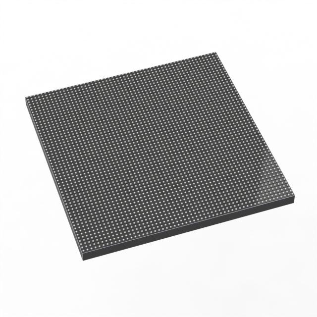
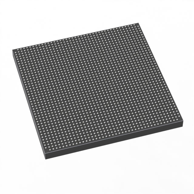
Stratix® 10 TX Field Programmable Gate Array (FPGA) IC 440 2500000 2397-BBGA, FCBGA |
|---|---|
| Quantity | 599 Available (as of June 15, 2026) |

| Product Category | Field Programmable Gate Array (FPGA) |
|---|---|
| Manufacturer | Intel |
| Manufacturing Status | Active |
| Manufacturer Standard Lead Time | 12 Weeks |
| Datasheet |
Specifications & Environmental
| Device Package | 2397-FBGA, FC (50x50) | Grade | Extended | Operating Temperature | 0°C – 100°C | ||
|---|---|---|---|---|---|---|---|
| Package / Case | 2397-BBGA, FCBGA | Number of I/O | 440 | Voltage | 820 mV - 880 mV | ||
| Mounting Method | Surface Mount | RoHS Compliance | Unknown | REACH Compliance | REACH Unaffected | ||
| Moisture Sensitivity Level | 3 (168 Hours) | Number of LABs/CLBs | 312500 | Number of Logic Elements/Cells | 2500000 | ||
| Number of Gates | N/A | ECCN | N/A | HTS Code | N/A | ||
| Qualification | N/A | Total RAM Bits | 204472320 |
Overview of 1ST250EU3F50E3XG – Stratix® 10 TX Field Programmable Gate Array (FPGA)
The 1ST250EU3F50E3XG is an Intel Stratix® 10 TX FPGA in a high-density FCBGA package, delivering up to 2,500,000 logic elements and 204,472,320 bits of on‑chip RAM. Built for designs that require very large programmable fabric, extensive memory, and substantial I/O bandwidth, this device targets high-performance communications, data center, and compute-acceleration systems.
Based on the Stratix 10 TX family architecture, the device benefits from the series’ advanced core innovations (including the Intel HyperFlex® core architecture and heterogeneous packaging approaches described in the device overview), while offering a large I/O complement and a low-voltage core supply for power-optimized system integration.
Key Features
- Logic Capacity Provides 2,500,000 logic elements to implement large, complex FPGA designs and high-density custom logic.
- On‑Chip Memory Total RAM of 204,472,320 bits to support large buffering, packet processing, and on‑chip data structures.
- High‑Speed I/O 440 I/O pins support broad external connectivity for interfaces, memory, and high-speed links.
- Advanced Transceiver and Fabric Innovations Part of the Stratix 10 TX family which includes the HyperFlex core architecture and high-performance transceiver technology described in the device overview.
- Power and Voltage Core supply voltage range specified at 820 mV to 880 mV for system power planning and regulator selection.
- Package and Mounting 2397‑BBGA (FCBGA) package; supplier device package listed as 2397‑FBGA, FC (50×50). Surface-mount mounting type supports standard PCB assembly flows.
- Operating Range and Grade Extended grade device with an operating temperature range of 0 °C to 100 °C suitable for controlled-environment, high-performance systems.
- Compliance RoHS‑compliant for environmental regulatory considerations.
Typical Applications
- High‑Bandwidth Networking Used in line cards and switch fabric applications where large logic capacity and high aggregate I/O bandwidth are required.
- Data Center Acceleration Implements custom acceleration pipelines, packet processing, and large on‑chip memory buffers for low‑latency compute tasks.
- Telecommunications Equipment Supports systems that need programmable protocol handling and flexible I/O bandwidth for next‑generation transport links.
- High‑Performance Test & Measurement Deploys large logic designs and substantial RAM for real‑time signal processing and data capture workloads.
Unique Advantages
- High Logic Density: 2,500,000 logic elements enable integration of large systems on a single device, reducing the need for multiple FPGAs.
- Large On‑Chip Memory: 204,472,320 bits of RAM provide ample capacity for buffering, packet queues, and dataflow acceleration without immediate external memory dependence.
- Broad I/O Count: 440 I/Os accommodate multiple interfaces and parallel external devices for flexible board-level integration.
- Power‑Optimized Core Supply: Narrow core voltage range (820 mV–880 mV) supports efficient power delivery and regulator selection for dense systems.
- FCBGA Packaging: 2397‑FBGA/BBGA package in a 50×50 form factor supports high-pin-count, high-density PCB layouts while maintaining surface-mount assembly compatibility.
- Extended Temperature Grade: Rated for 0 °C to 100 °C operation to meet the requirements of many high-performance electronic systems.
Why Choose 1ST250EU3F50E3XG?
The 1ST250EU3F50E3XG positions itself as a high-capacity Stratix 10 TX FPGA for designs that demand substantial programmable logic, significant on‑chip memory, and extensive I/O. Its specifications—2.5 million logic elements, over 204 million bits of RAM, and 440 I/Os—make it suitable for complex networking, acceleration, and telecommunication platforms where consolidation of functions into a single, scalable device reduces board complexity.
As part of the Stratix 10 TX family, this device aligns with a product line engineered for high aggregate bandwidth and advanced fabric features, providing a pathway for scalable designs that require long-term performance and integration headroom.
Request a quote or submit a procurement inquiry to evaluate 1ST250EU3F50E3XG for your next high-performance FPGA design.


Date Founded: 1968
Headquarters: Santa Clara, California, USA
Employees: 130,000+
Revenue: $54.23 Billion
Certifications and Memberships: ISO9001:2015, ISO14001:2015, ISO17025:2017, ISO27001:2022, ISO45001:2018, ISO50001:2018


