
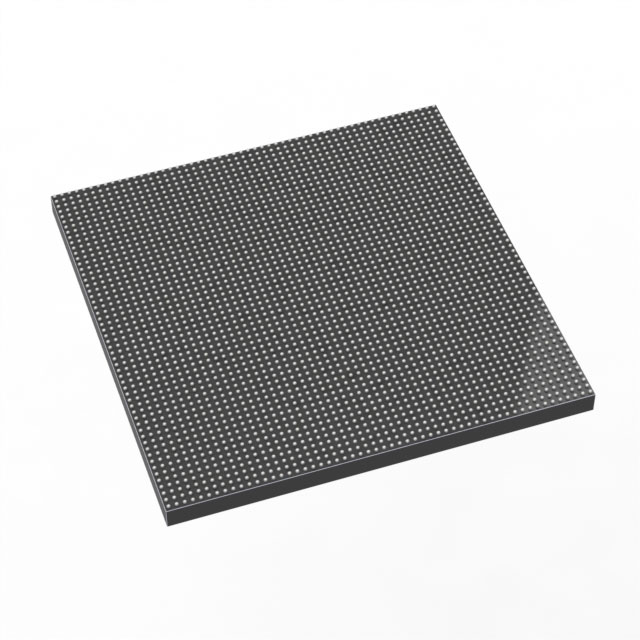
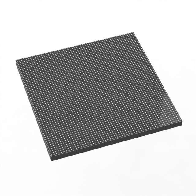
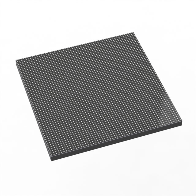
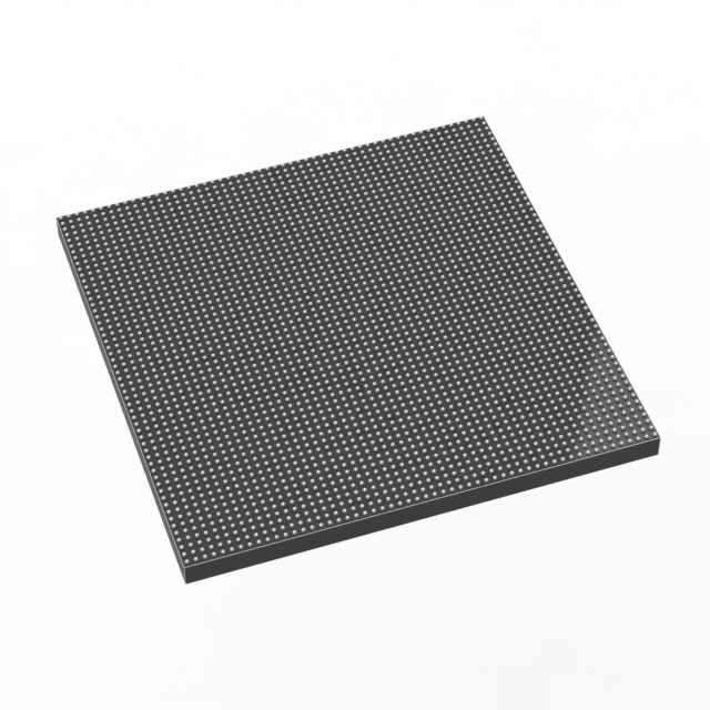
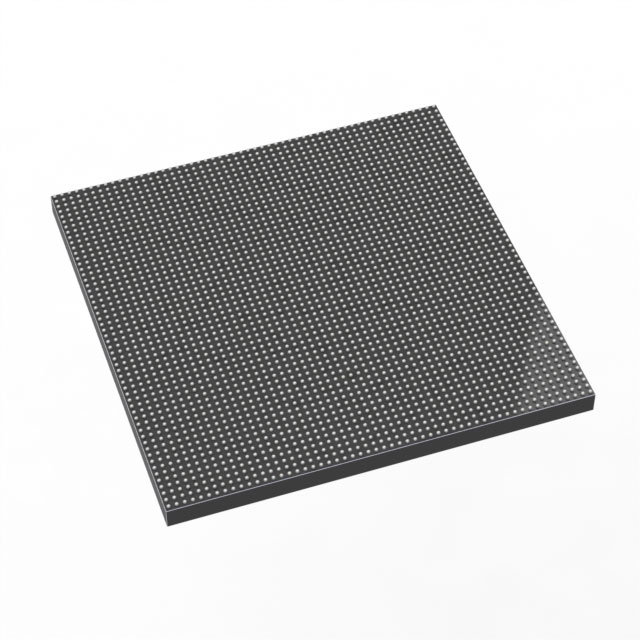
1ST280EY2F55E1VG
| Part Description |
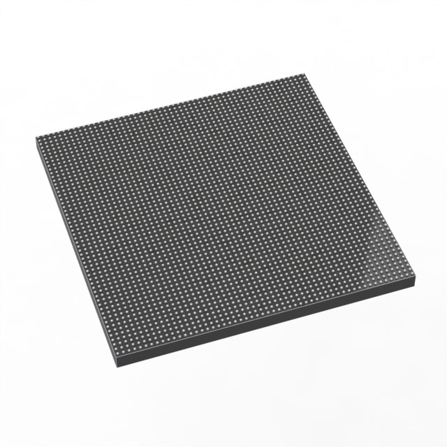
Stratix® 10 TX Field Programmable Gate Array (FPGA) IC 296 2800000 2912-BBGA, FCBGA |
|---|---|
| Quantity | 839 Available (as of October 8, 2026) |
| Product Category | Field Programmable Gate Array (FPGA) |
|---|---|
| Manufacturer | Intel |
| Manufacturing Status | Active |
| Manufacturer Standard Lead Time | 12 Weeks |
| Datasheet |
Specifications & Environmental
| Device Package | 2912-FBGA, FC (55x55) | Grade | Extended | Operating Temperature | 0°C – 100°C | ||
|---|---|---|---|---|---|---|---|
| Package / Case | 2912-BBGA, FCBGA | Number of I/O | 296 | Voltage | 770 mV - 970 mV | ||
| Mounting Method | Surface Mount | RoHS Compliance | Unknown | REACH Compliance | REACH Unaffected | ||
| Moisture Sensitivity Level | 3 (168 Hours) | Number of LABs/CLBs | 350000 | Number of Logic Elements/Cells | 2800000 | ||
| Number of Gates | N/A | ECCN | N/A | HTS Code | N/A | ||
| Qualification | N/A | Total RAM Bits | 240123904 |
Overview of 1ST280EY2F55E1VG – Stratix® 10 TX Field Programmable Gate Array (FPGA), 2.8M Logic Elements, 296 I/O, 2912‑BBGA
The 1ST280EY2F55E1VG is a Stratix® 10 TX FPGA device in a 2912‑BBGA surface‑mount package, offering 2,800,000 logic elements and 296 general‑purpose I/O. It is built on the Stratix 10 TX architecture and HyperFlex core innovations described in the device overview.
Designed for high‑bandwidth, high‑integration systems, this device supports advanced transceiver and hardened IP features at the device‑level and targets applications that require large programmable fabric, extensive on‑chip memory, and dense I/O in a single FCBGA package.
Key Features
- Core & Architecture HyperFlex® core architecture is referenced in the device overview and underpins the Stratix 10 TX family’s high‑performance programmable fabric.
- Logic Capacity 2,800,000 logic elements (LEs) provide a very large programmable fabric suitable for complex logic, packet processing, and heavy compute offload.
- Memory Total on‑chip RAM of 240,123,904 bits enables large buffering and on‑chip data storage for DSP, networking, and packet buffering functions.
- High‑Speed I/O & Transceivers Device overview documents dual‑mode transceivers with support in the Stratix 10 TX family for PAM4 and NRZ operation and family transceiver capabilities up to multi‑Gbps rates for high‑bandwidth links.
- Hardened IP The Stratix 10 TX family overview references hardened PCI Express Gen3 and Ethernet MAC IP blocks and dedicated FEC options for high‑throughput data connectivity.
- Embedded Processing Options The family overview describes an embedded Hard Processor System (HPS) available on select devices, enabling application‑class processing alongside programmable fabric.
- Power and Operating Range Supported supply voltage range is 770 mV to 970 mV, with an operating temperature range of 0 °C to 100 °C suitable for extended‑grade environments.
- Package & Mounting Surface‑mount 2912‑BBGA (2912‑FBGA, FC 55×55) package provides a compact, high‑pin‑count solution for system integration; 296 I/O pins enable dense external connectivity.
- Standards & Compliance RoHS‑compliant material status is provided for compliance with common environmental regulations.
Typical Applications
- High‑bandwidth Networking Large logic capacity, extensive on‑chip RAM, and high‑speed transceiver capabilities enable packet processing, switching, and MAC/FEC acceleration for network equipment.
- Telecom & Data Center Interconnect Dual‑mode transceiver support and hardened Ethernet/PCIe IP referenced in the device family make this device suitable for backplane and chip‑to‑chip high‑speed links.
- Compute Acceleration Large programmable fabric and memory resources support custom accelerators and DSP pipelines for data‑plane and compute offload tasks.
Unique Advantages
- Very large programmable fabric: 2,800,000 logic elements provide headroom for complex designs and multi‑function implementations.
- Substantial on‑chip memory: 240,123,904 total RAM bits reduce reliance on external memory for buffering and stateful processing.
- High I/O density in a compact package: 296 I/O in a 2912‑BBGA FCBGA package delivers extensive connectivity while minimizing board area.
- Device‑level power parameters: Specified supply voltage range (770 mV–970 mV) allows designers to plan power delivery and power domains accurately.
- Extended‑grade operating range: Rated for 0 °C to 100 °C operation to meet extended commercial environment requirements.
- RoHS compliant: Materials compliance supports environmental and regulatory requirements.
Why Choose 1ST280EY2F55E1VG?
The 1ST280EY2F55E1VG combines a very large Stratix 10 TX programmable fabric with extensive on‑chip memory and dense I/O in a 2912‑BBGA package. It is positioned for system designs requiring high logic capacity, significant local memory, and high‑speed connectivity options described for the Stratix 10 TX family.
Engineers developing networking, telecom interconnect, and compute‑acceleration solutions will find this device’s balance of logic, memory, I/O, and device‑level power and thermal specifications suitable for complex, high‑integration designs in extended‑grade environments.
Request a quote or submit an inquiry to obtain pricing, availability, and additional technical details for 1ST280EY2F55E1VG. Our team can provide configuration, lead‑time, and ordering assistance tailored to your project needs.





















Date Founded: 1968
Headquarters: Santa Clara, California, USA
Employees: 130,000+
Revenue: $54.23 Billion
Certifications and Memberships: ISO9001:2015, ISO14001:2015, ISO17025:2017, ISO27001:2022, ISO45001:2018, ISO50001:2018


