
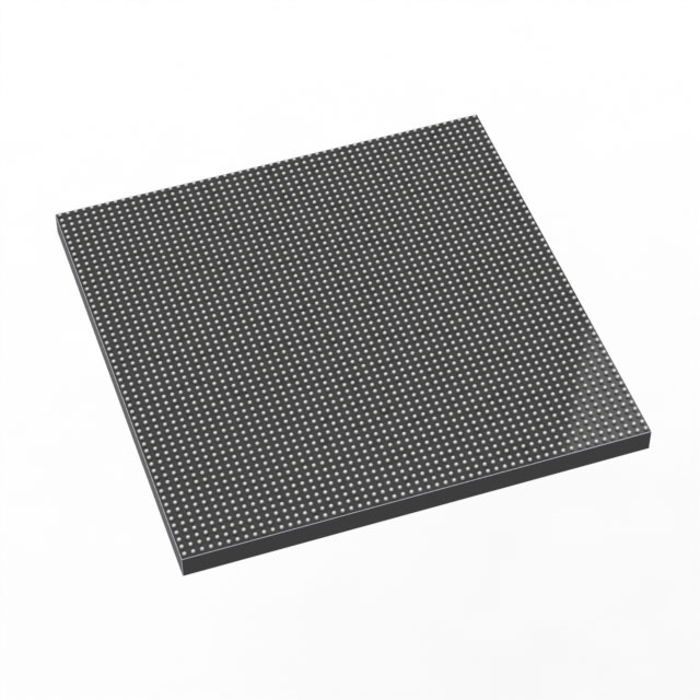
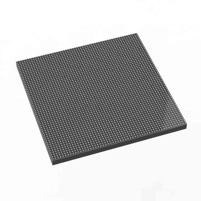
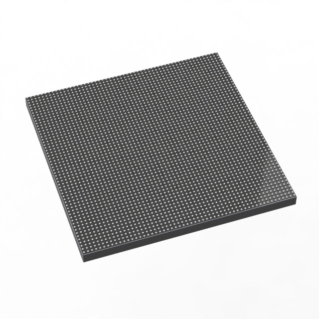
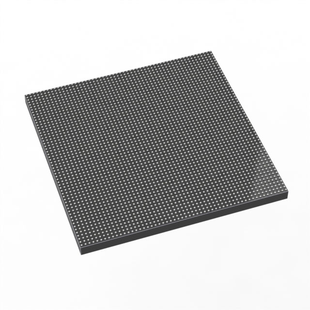
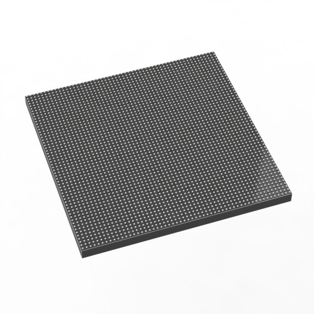
1ST280EY2F55E2LG
| Part Description |
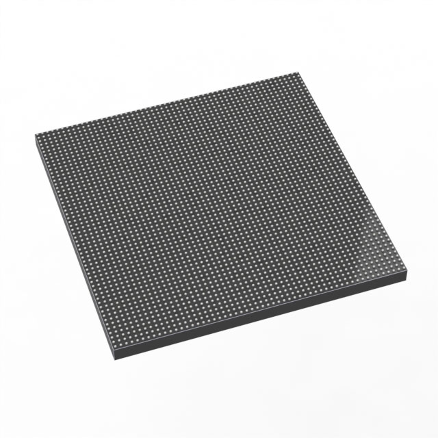
Stratix® 10 TX Field Programmable Gate Array (FPGA) IC 296 2800000 2912-BBGA, FCBGA |
|---|---|
| Quantity | 115 Available (as of October 8, 2026) |
| Product Category | Field Programmable Gate Array (FPGA) |
|---|---|
| Manufacturer | Intel |
| Manufacturing Status | Active |
| Manufacturer Standard Lead Time | 12 Weeks |
| Datasheet |
Specifications & Environmental
| Device Package | 2912-FBGA, FC (55x55) | Grade | Extended | Operating Temperature | 0°C – 100°C | ||
|---|---|---|---|---|---|---|---|
| Package / Case | 2912-BBGA, FCBGA | Number of I/O | 296 | Voltage | 820 mV - 880 mV | ||
| Mounting Method | Surface Mount | RoHS Compliance | Unknown | REACH Compliance | REACH Unaffected | ||
| Moisture Sensitivity Level | 3 (168 Hours) | Number of LABs/CLBs | 350000 | Number of Logic Elements/Cells | 2800000 | ||
| Number of Gates | N/A | ECCN | N/A | HTS Code | N/A | ||
| Qualification | N/A | Total RAM Bits | 240123904 |
Overview of 1ST280EY2F55E2LG – Stratix® 10 TX FPGA, 2.8M Logic Elements, 2912-BBGA
The 1ST280EY2F55E2LG is an Intel Stratix® 10 TX field programmable gate array (FPGA) in a 2912-ball FCBGA package. It integrates a high-performance HyperFlex® core fabric with dense programmable logic and large on-chip RAM to address demanding, high-bandwidth system designs.
Built for applications that require high transceiver bandwidth, hardened protocol IP, and scalable logic capacity, this device targets next-generation networking, compute, and interconnect use cases where performance, integration, and power efficiency matter.
Key Features
- Logic Capacity 2,800,000 logic elements (LEs) to implement large, complex designs and custom hardware acceleration.
- On‑Chip Memory 240,123,904 total RAM bits for high-density buffering, packet processing, and large working sets.
- I/O and Packaging 296 I/Os in a surface-mount 2912-BBGA (2912-FBGA, FC 55×55) package for dense board-level integration.
- High‑Speed Transceivers Dual-mode transceivers supporting PAM4 up to 57.8 Gbps and NRZ up to 28.9 Gbps, suitable for chip-to-chip, chip-to-module, and backplane links as described in the device overview.
- Hardened Protocol IP Includes hardened PCI Express Gen3 and 10/25/100 Gbps Ethernet MAC IP blocks and dedicated Reed‑Solomon FEC options referenced in the device overview.
- Advanced Core Architecture Intel HyperFlex® core architecture and 14 nm FinFET process technology are documented in the device overview for improved core performance.
- Embedded Processor Option Select devices in the Stratix 10 TX family include an embedded quad-core 64-bit Arm Cortex‑A53 hard processor system (HPS), according to the datasheet overview.
- Clocking and PLLs Fractional synthesis and ultra-low jitter PLL architectures are included for precision clocking in high-speed designs.
- Power and Voltage Specified core supply voltage range 820 mV to 880 mV to match system power design requirements.
- Operating Range and Grade Extended grade with an operating temperature range of 0 °C to 100 °C.
- Reliability and Packaging Technology Monolithic core fabric combined with heterogeneous 3D SiP transceiver tiles and EMIB packaging innovations are described in the device overview to support high-bandwidth integration.
Typical Applications
- High‑Speed Networking and Data Center Interconnects Leverages multi‑Gbps transceivers and hardened Ethernet MAC IP for packet processing, switching, and line-rate forwarding.
- Backplane and Chip‑to‑Module Links Dual-mode transceivers (PAM4/NRZ) and high I/O density support chip-to-chip, module, and backplane connectivity.
- PCI Express System Accelerators Hardened PCIe Gen3 IP enables integration into accelerator cards and host-attached subsystems requiring PCIe connectivity.
- Custom Compute and DSP Large logic capacity and abundant on-chip RAM support custom hardware acceleration, signal processing, and data-path implementations.
Unique Advantages
- High Aggregate Bandwidth: The device family delivers multi‑Tbps transceiver bandwidth as documented in the device overview, addressing demanding link-rate requirements.
- Large, Scalable Fabric: 2.8 million logic elements and extensive on‑chip RAM provide the capacity to consolidate multiple system functions into a single FPGA.
- Integrated Protocol IP: Hardened PCIe and Ethernet MAC IP reduce development time and lower implementation risk for standard interfaces.
- Advanced Packaging: Monolithic core fabric combined with heterogeneous SiP transceiver tiles and EMIB packaging supports high-density integration and high-speed I/O.
- Precise Clocking and PLLs: Fractional synthesis and low-jitter PLLs support stringent timing and jitter-sensitive high-speed links.
- Extended Temperature Grade: 0 °C to 100 °C operating range supports deployment in thermally demanding systems.
Why Choose 1ST280EY2F55E2LG?
The 1ST280EY2F55E2LG combines a high-capacity HyperFlex® FPGA fabric with advanced transceiver technology and hardened protocol IP to address high-bandwidth, low-latency system requirements. Its dense logic, large on‑chip memory, and packaged transceiver tiles are suited for designers building scalable networking, compute acceleration, and interconnect solutions.
Backed by Intel's Stratix 10 TX device architecture and packaging innovations described in the product overview, this device is intended for teams seeking a high-performance, integrated FPGA platform that supports complex, bandwidth‑intensive designs with precise clocking and proven protocol blocks.
Request a quote or submit an inquiry for 1ST280EY2F55E2LG to receive availability and pricing information.





















Date Founded: 1968
Headquarters: Santa Clara, California, USA
Employees: 130,000+
Revenue: $54.23 Billion
Certifications and Memberships: ISO9001:2015, ISO14001:2015, ISO17025:2017, ISO27001:2022, ISO45001:2018, ISO50001:2018


