
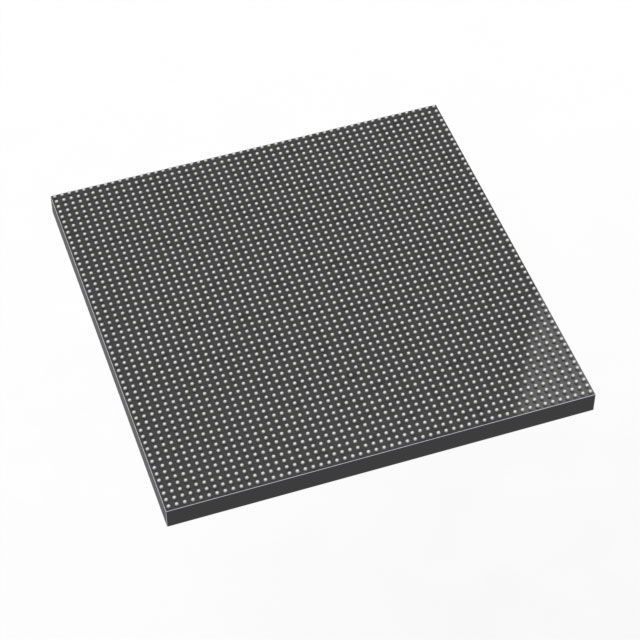
1ST280EY2F55I1VG
| Part Description |
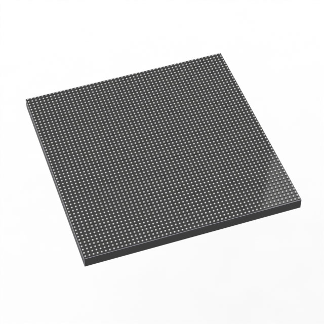
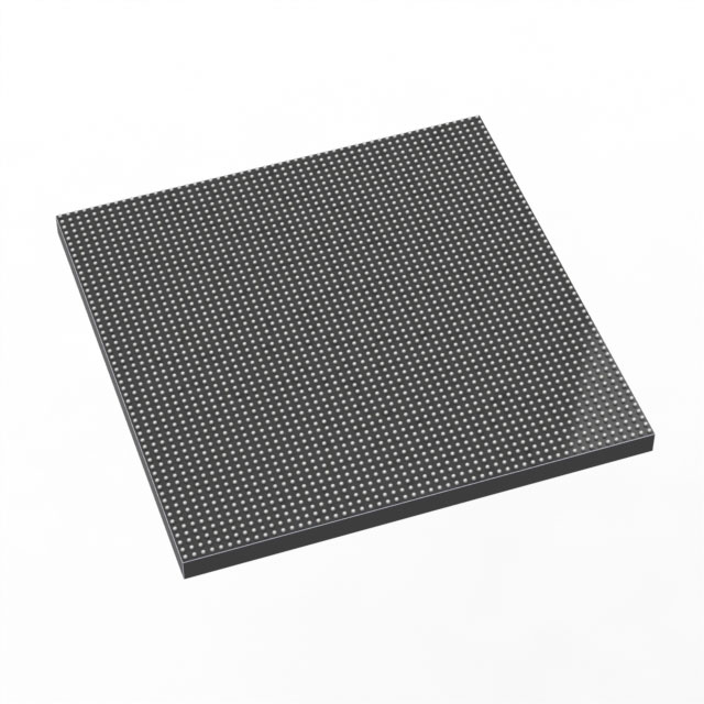
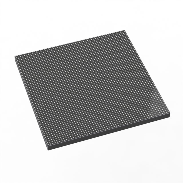
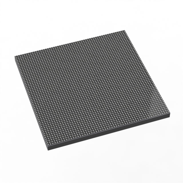
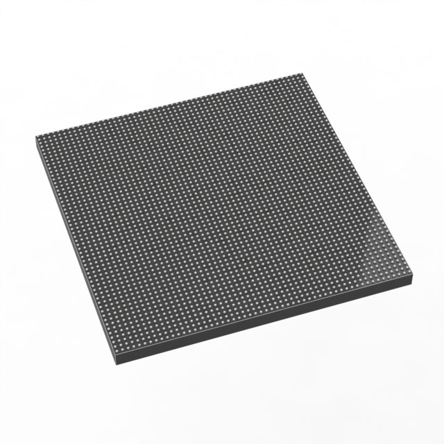
Stratix® 10 TX Field Programmable Gate Array (FPGA) IC 296 2800000 2912-BBGA, FCBGA |
|---|---|
| Quantity | 538 Available (as of October 8, 2026) |
| Product Category | Field Programmable Gate Array (FPGA) |
|---|---|
| Manufacturer | Intel |
| Manufacturing Status | Active |
| Manufacturer Standard Lead Time | 12 Weeks |
| Datasheet |
Specifications & Environmental
| Device Package | 2912-FBGA, FC (55x55) | Grade | Industrial | Operating Temperature | -40°C – 100°C | ||
|---|---|---|---|---|---|---|---|
| Package / Case | 2912-BBGA, FCBGA | Number of I/O | 296 | Voltage | 770 mV - 970 mV | ||
| Mounting Method | Surface Mount | RoHS Compliance | Unknown | REACH Compliance | REACH Unaffected | ||
| Moisture Sensitivity Level | 3 (168 Hours) | Number of LABs/CLBs | 350000 | Number of Logic Elements/Cells | 2800000 | ||
| Number of Gates | N/A | ECCN | N/A | HTS Code | N/A | ||
| Qualification | N/A | Total RAM Bits | 240123904 |
Overview of 1ST280EY2F55I1VG – Stratix® 10 TX FPGA, 2,800,000 logic elements, 2912-BBGA
The 1ST280EY2F55I1VG is an Intel Stratix® 10 TX field programmable gate array (FPGA) supplied in a 2912-BBGA (FCBGA) surface-mount package. It integrates a monolithic 14 nm FPGA fabric with high‑speed heterogeneous transceiver tiles and advanced packaging technology.
Designed for high-bandwidth communications and compute‑intensive designs, this device combines a HyperFlex® core architecture, dual‑mode transceivers, hardened IP blocks and an optional embedded hard processor system to deliver large logic capacity, large internal RAM, and flexible I/O within an industrial temperature grade.
Key Features
- Large programmable fabric — 2,800,000 logic elements (LEs) providing substantial logic capacity for complex designs.
- On-chip memory — 240,123,904 total RAM bits to support large buffering, packet processing, and algorithmic workloads.
- High‑speed transceivers — Dual‑mode transceivers capable of both 57.8 Gbps PAM4 and 28.9 Gbps NRZ operation, and up to 144 full-duplex channels as described in the device family overview.
- Hardened interfaces — Integrated hard PCI Express Gen3 and 10/25/100 Gbps Ethernet MAC options with dedicated FEC support as documented for the Stratix 10 TX family.
- Advanced core architecture — Intel HyperFlex® core architecture designed to increase core performance compared to previous generations (per device family documentation).
- Embedded processing (select devices) — Quad-core 64-bit Arm Cortex‑A53 hard processor system (HPS) available in select Stratix 10 TX devices for application-class processing.
- Power and clocking — Core voltage supply range of 770 mV to 970 mV with fractional synthesis and low-jitter PLLs described in the device overview.
- Industrial grade — Rated for operation from −40 °C to 100 °C.
- Package and I/O — 2912‑BBGA (2912‑FBGA, 55×55 FC variant listed) surface-mount package with 296 I/O pins.
- Reliability and packaging technology — Heterogeneous 3D SiP transceiver tiles and Intel Embedded Multi‑die Interconnect Bridge (EMIB) technology described for the family.
Typical Applications
- High‑bandwidth networking and telecom — Dual‑mode transceivers and hardened Ethernet MAC/FEC support enable line‑rate packet processing and backbone transport implementations.
- Data center and cloud interconnect — Large logic capacity, high aggregate transceiver bandwidth and PCIe hard IP make the device suitable for switch, NIC, and accelerator interface designs.
- Backplane and chip‑to‑chip systems — Multi‑channel 28.9 Gbps NRZ or 57.8 Gbps PAM4 transceiver operation supports high‑speed chip‑to‑module and backplane links.
- Compute acceleration and signal processing — Extensive RAM and logic resources, plus hardened DSP and optional HPS, support dataflow acceleration and algorithmic workloads.
- Test & measurement and prototyping — Flexible I/O, high logic density, and advanced clocking PLLs support complex test instrumentation and high‑speed prototyping tasks.
Unique Advantages
- High logic density — 2.8 million logic elements enable integration of large, complex functions into a single device, reducing board-level partitioning.
- Extensive on-chip memory — 240,123,904 bits of RAM support large buffers and stateful processing without immediate reliance on external memory.
- Flexible, high‑speed I/O — Dual‑mode transceivers and up to 144 full‑duplex channels provide adaptable link options for both PAM4 and NRZ systems.
- Industrial temperature rating — −40 °C to 100 °C operating range fits designs targeting harsh or wide‑range environments.
- Advanced packaging and integration — Heterogeneous 3D SiP tiles and EMIB packaging allow high-bandwidth integration while keeping a single flip‑chip BGA footprint.
- Integrated system capabilities — Hardened PCIe and Ethernet MAC IP, plus optional quad‑core Arm Cortex‑A53 HPS, help consolidate system functions and reduce external components.
Why Choose 1ST280EY2F55I1VG?
The 1ST280EY2F55I1VG brings a high‑capacity Stratix 10 TX FPGA into a 2912‑ball FCBGA package, combining 2.8 million logic elements, substantial internal RAM, and industrial temperature operation for demanding designs. Its mix of advanced HyperFlex® fabric, high‑speed transceivers, hardened interface IP and modern packaging makes it a strong option for designers who need integrated bandwidth, logic scale, and robust system features in a single FPGA device.
This device is well suited to teams building high‑performance networking, data center interconnect, backplane or compute‑acceleration hardware that benefit from consolidated functionality, scalable logic resources, and flexible high‑speed I/O options provided by the Stratix 10 TX family.
Request a quote or submit a sales inquiry to receive pricing and availability details for 1ST280EY2F55I1VG.





















Date Founded: 1968
Headquarters: Santa Clara, California, USA
Employees: 130,000+
Revenue: $54.23 Billion
Certifications and Memberships: ISO9001:2015, ISO14001:2015, ISO17025:2017, ISO27001:2022, ISO45001:2018, ISO50001:2018


