
1ST280EY2F55I1VGAS
| Part Description |
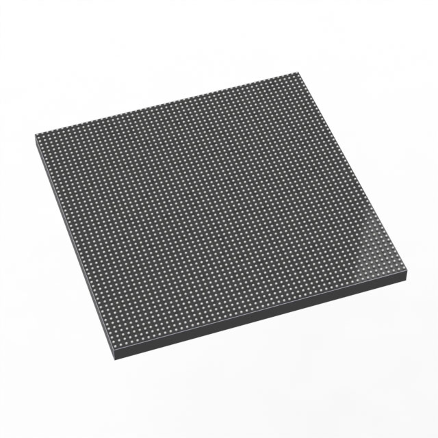
Stratix® 10 TX Field Programmable Gate Array (FPGA) IC 296 2800000 2912-BBGA, FCBGA |
|---|---|
| Quantity | 1,364 Available (as of June 15, 2026) |
| Product Category | Field Programmable Gate Array (FPGA) |
|---|---|
| Manufacturer | Intel |
| Manufacturing Status | Active |
| Manufacturer Standard Lead Time | 12 Weeks |
| Datasheet |
Specifications & Environmental
| Device Package | 2912-FBGA, FC (55x55) | Grade | Industrial | Operating Temperature | -40°C – 100°C | ||
|---|---|---|---|---|---|---|---|
| Package / Case | 2912-BBGA, FCBGA | Number of I/O | 296 | Voltage | 770 mV - 970 mV | ||
| Mounting Method | Surface Mount | RoHS Compliance | Unknown | REACH Compliance | REACH Unaffected | ||
| Moisture Sensitivity Level | 3 (168 Hours) | Number of LABs/CLBs | 350000 | Number of Logic Elements/Cells | 2800000 | ||
| Number of Gates | N/A | ECCN | N/A | HTS Code | N/A | ||
| Qualification | N/A | Total RAM Bits | 240123904 |
Overview of 1ST280EY2F55I1VGAS – Stratix® 10 TX FPGA (2912‑BBGA, FCBGA)
The 1ST280EY2F55I1VGAS is an Intel Stratix® 10 TX Field Programmable Gate Array in a 2912‑ball BGA (FCBGA) package. This industrial‑grade device delivers very high logic density and on‑chip memory alongside family‑level innovations such as the HyperFlex® core architecture and high‑speed dual‑mode transceivers.
With 2,800,000 logic elements, 240,123,904 bits of total RAM and 296 I/O pins, the device targets applications that demand large programmable fabric, heavy on‑chip memory, and high aggregate bandwidth — including networking, data center acceleration, and high‑performance communications systems.
Key Features
- Core & Architecture HyperFlex® core architecture (family feature) and Intel 14 nm tri‑gate technology; this specific device provides 2,800,000 logic elements for large, compute‑intensive FPGA designs.
- On‑Chip Memory 240,123,904 total RAM bits of on‑device memory, enabling large buffering and state storage for data‑plane and signal‑processing applications.
- High‑Speed Transceivers (Family‑Level) Stratix 10 TX family supports up to 144 full‑duplex transceiver channels with dual‑mode operation: up to 57.8 Gbps PAM4 and 28.9 Gbps NRZ, providing high aggregate bandwidth for backplane, chip‑to‑chip and module links.
- Hard IP & DSP (Family‑Level) Family features include hardened PCI Express Gen3 x16 and 10/25/100 Gbps Ethernet MAC with Reed‑Solomon FEC, plus hardened floating‑point DSP blocks for compute and packet processing acceleration.
- Package & I/O 2912‑BBGA (FCBGA) 55×55 supplier device package, surface‑mount, with 296 user I/O pins to support broad system connectivity.
- Power & Supply Core supply range specified at 770 mV to 970 mV, allowing system designers to plan accurate power delivery and thermal budgets.
- Industrial Temperature & Compliance Rated operating temperature of −40 °C to 100 °C and RoHS compliant for industrial use cases.
Typical Applications
- High‑Speed Networking Used in line cards and switches where large logic capacity and high transceiver bandwidth enable packet processing, MAC offload and FEC implementations.
- Data Center Acceleration Suitable for FPGA‑based accelerators and NICs that require dense logic, substantial on‑chip RAM and connectivity to high‑speed fabrics.
- Telecom & Optical Transport Employed in transport equipment and modules that need multi‑Gbps PAM4/NRZ links and scalable MAC/PCS implementations.
- High‑Performance Computing & Test Applied where heavy DSP and memory bandwidth are required for signal processing, emulation, or hardware verification platforms.
Unique Advantages
- Very high logic density: 2,800,000 logic elements accommodate large, complex designs without partitioning across multiple devices.
- Large on‑chip memory: 240,123,904 bits of RAM reduce external memory dependencies and improve latency for buffering and stateful processing.
- Family‑level high aggregate bandwidth: Dual‑mode transceivers and up to 144 channels (family capability) enable multi‑terabit system architectures.
- Industrial temperature rating: −40 °C to 100 °C operating range supports deployment in harsh and temperature‑variable environments.
- Compact, manufacturable package: 2912‑ball FCBGA surface‑mount package balances high I/O count with standard PCB assembly processes.
Why Choose 1ST280EY2F55I1VGAS?
This Stratix 10 TX device combines extremely high logic capacity, substantial embedded memory, and the connectivity required for high‑bandwidth systems in an industrial‑rated package. It is positioned for system designers building scalable networking, acceleration, and communications equipment who need large programmable fabric and predictable electrical and thermal planning.
Choosing this device provides a path to consolidate complex functions into a single FPGA with robust I/O, family‑level transceiver capabilities, and the legacy of Intel Stratix 10 TX architectural features — all of which support long‑term design scalability and integration in demanding applications.
Request a quote or submit an RFQ to get pricing, availability and lead‑time information for 1ST280EY2F55I1VGAS.


Date Founded: 1968
Headquarters: Santa Clara, California, USA
Employees: 130,000+
Revenue: $54.23 Billion
Certifications and Memberships: ISO9001:2015, ISO14001:2015, ISO17025:2017, ISO27001:2022, ISO45001:2018, ISO50001:2018


