
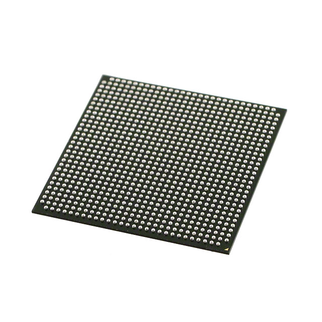
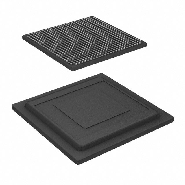
5AGXMA3D4F27C5N
| Part Description |
Arria V GX Field Programmable Gate Array (FPGA) IC 336 11746304 156000 672-BBGA, FCBGA |
|---|---|
| Quantity | 887 Available (as of June 15, 2026) |

| Product Category | Field Programmable Gate Array (FPGA) |
|---|---|
| Manufacturer | Intel |
| Manufacturing Status | Obsolete |
| Manufacturer Standard Lead Time | Contact Us |
| Datasheet |
Specifications & Environmental
| Device Package | 672-FBGA (27x27) | Grade | Commercial | Operating Temperature | 0°C – 85°C | ||
|---|---|---|---|---|---|---|---|
| Package / Case | 672-BBGA, FCBGA | Number of I/O | 336 | Voltage | 1.07 V - 1.13 V | ||
| Mounting Method | Surface Mount | RoHS Compliance | RoHS Compliant | REACH Compliance | REACH Unknown | ||
| Moisture Sensitivity Level | 3 (168 Hours) | Number of LABs/CLBs | 7362 | Number of Logic Elements/Cells | 156000 | ||
| Number of Gates | N/A | ECCN | 3A001A2C | HTS Code | 8542.39.0001 | ||
| Qualification | N/A | Total RAM Bits | 11746304 |
Overview of 5AGXMA3D4F27C5N – Arria V GX FPGA, 156,000 Logic Elements, 672‑FBGA
The 5AGXMA3D4F27C5N is an Intel Arria V GX Field Programmable Gate Array (FPGA) offered in a 672‑FBGA (27×27) FCBGA package. It delivers a high logic capacity and embedded on‑chip memory in a surface‑mount package designed for commercial‑grade applications.
Key attributes—including 156,000 logic elements, approximately 11.75 Mbits of embedded memory, and 336 I/O—make this device suitable for designs that require substantial logic density, on‑chip RAM, and broad I/O connectivity within a compact BGA footprint.
Key Features
- Core Logic 156,000 logic elements provide substantial resources for complex logic implementation and custom hardware acceleration.
- Embedded Memory Approximately 11.75 Mbits of on‑chip RAM to support buffering, state storage, and memory‑intensive logic functions.
- I/O Capacity 336 programmable I/O pins for flexible interfacing to peripherals, memory, and system buses.
- Packaging 672‑BBGA FCBGA package (supplier package: 672‑FBGA, 27×27) in a surface‑mount form factor for compact PCB integration.
- Power Core voltage supply specified at 1.07 V to 1.13 V to match system power design requirements.
- Operating Range Commercial grade operation from 0 °C to 85 °C for typical commercial embedded environments.
- Compliance RoHS‑compliant manufacturing to meet environmental and assembly standards.
Typical Applications
- Logic‑dense FPGA designs Use the device where a large number of logic elements are needed to implement complex, custom digital functions.
- Memory‑intensive processing Leverage approximately 11.75 Mbits of embedded memory for buffering, packet processing, or large state machines.
- I/O‑rich systems Deploy in systems that require hundreds of I/O signals to interface with sensors, peripherals, or external memory devices.
- Compact PCB implementations The 672‑FBGA package supports high‑density board layouts and surface‑mount assembly for space‑constrained designs.
Unique Advantages
- High logic capacity: 156,000 logic elements enable implementation of complex digital functions without external logic expansion.
- Substantial on‑chip RAM: Approximately 11.75 Mbits of embedded memory reduces reliance on external memory for many applications.
- Extensive I/O: 336 I/O pins provide flexibility to support diverse peripheral and bus interfaces directly from the FPGA.
- Compact, manufacturable package: 672‑FBGA (27×27) FCBGA surface‑mount package simplifies PCB routing while supporting automated assembly.
- Commercial temperature rating: Specified operation from 0 °C to 85 °C aligns with standard commercial electronic environments.
- RoHS compliant: Environmentally compliant manufacturing facilitates global assembly and distribution requirements.
Why Choose 5AGXMA3D4F27C5N?
The 5AGXMA3D4F27C5N Arria V GX FPGA balances high logic density, significant embedded memory, and broad I/O capability inside a compact 672‑FBGA surface‑mount package. It is positioned for commercial designs that require large programmable fabric and on‑chip RAM while maintaining a compact board footprint and standard temperature range.
Supported by Intel Arria V device documentation, this part is appropriate for teams seeking a verified FPGA device with clearly specified electrical, timing, and configuration characteristics for reliable integration into mid‑ to high‑complexity systems.
Request a quote or submit an inquiry for pricing and availability to move your design forward with the 5AGXMA3D4F27C5N Arria V GX FPGA.


Date Founded: 1968
Headquarters: Santa Clara, California, USA
Employees: 130,000+
Revenue: $54.23 Billion
Certifications and Memberships: ISO9001:2015, ISO14001:2015, ISO17025:2017, ISO27001:2022, ISO45001:2018, ISO50001:2018


