
5AGXMA3D4F27C4N
| Part Description |
Arria V GX Field Programmable Gate Array (FPGA) IC 336 11746304 156000 672-BBGA, FCBGA |
|---|---|
| Quantity | 451 Available (as of June 10, 2026) |

| Product Category | Field Programmable Gate Array (FPGA) |
|---|---|
| Manufacturer | Intel |
| Manufacturing Status | Obsolete |
| Manufacturer Standard Lead Time | Contact Us |
| Datasheet |
Specifications & Environmental
| Device Package | 672-FBGA (27x27) | Grade | Commercial | Operating Temperature | 0°C – 85°C | ||
|---|---|---|---|---|---|---|---|
| Package / Case | 672-BBGA, FCBGA | Number of I/O | 336 | Voltage | 1.07 V - 1.13 V | ||
| Mounting Method | Surface Mount | RoHS Compliance | RoHS Compliant | REACH Compliance | REACH Unknown | ||
| Moisture Sensitivity Level | 3 (168 Hours) | Number of LABs/CLBs | 7362 | Number of Logic Elements/Cells | 156000 | ||
| Number of Gates | N/A | ECCN | 3A001A2C | HTS Code | 8542.39.0001 | ||
| Qualification | N/A | Total RAM Bits | 11746304 |
Overview of 5AGXMA3D4F27C4N – Arria V GX Field Programmable Gate Array (FPGA) IC
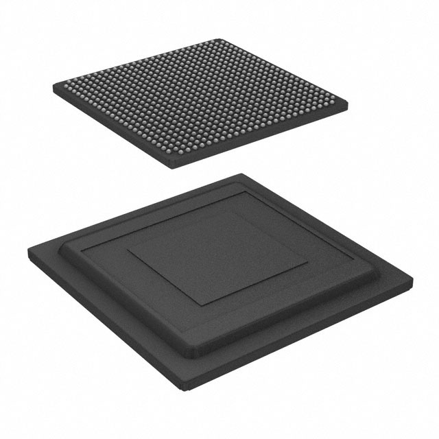
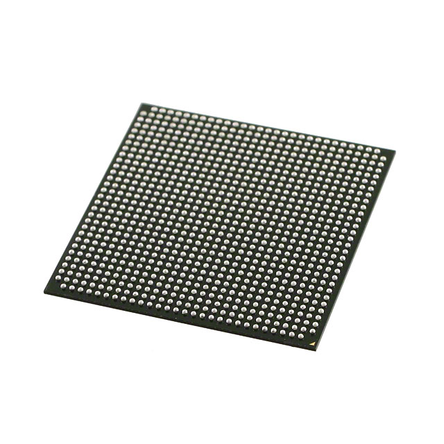
The 5AGXMA3D4F27C4N is an Arria V GX Field Programmable Gate Array (FPGA) delivered in a 672-ball BGA package. It provides a high-density programmable logic fabric with substantial on-chip RAM and a large I/O count for demanding digital designs.
Designed for commercial-grade applications, this device combines 156,000 logic elements and approximately 11.7 Mbits of embedded memory with 336 user I/Os, making it suitable for systems that require significant logic capacity, memory resources, and board-level I/O density.
Key Features
- Programmable Logic Capacity 156,000 logic elements provide extensive resources for complex fabric implementations.
- Logic Array Blocks 7,362 logic array blocks (LABs) to organize logic efficiently for synthesis and place-and-route.
- Embedded Memory Total on-chip RAM of 11,746,304 bits — approximately 11.7 Mbits of embedded memory for buffering, FIFOs, and local storage.
- I/O Density 336 user I/Os to support broad interfacing and parallel connectivity on modern PCBs.
- Package Options 672-BBGA, FCBGA package (supplier package: 672-FBGA, 27×27 mm) optimized for surface-mount assembly.
- Power Supply Range Core voltage supply specified from 1.07 V to 1.13 V to match system power delivery requirements.
- Operating Temperature Commercial operating range from 0 °C to 85 °C for standard temperature environment deployments.
- Mounting & Compliance Surface-mount device construction with RoHS compliance for assembly and environmental requirements.
Typical Applications
- High-density digital processing Use the device where large logic capacity and embedded memory are needed to implement custom datapaths, protocol handling, or control logic.
- Interface aggregation Leverage 336 I/Os for aggregating multiple parallel or serial interfaces at the board level.
- Prototyping and system integration Deploy as a programmable platform for validating ASIC-ready logic or integrating custom accelerators with significant on-chip resources.
Unique Advantages
- Substantial on-chip resources: 156,000 logic elements and approximately 11.7 Mbits of embedded memory reduce reliance on external logic and memory components.
- High I/O count: 336 user I/Os simplify board routing and support multiple peripheral connections without external expanders.
- Compact BGA packaging: 672-ball FCBGA (27×27) package balances high pin count with a compact footprint for space-constrained designs.
- Commercial-grade specification: Rated for 0 °C to 85 °C operation and RoHS compliant for standard commercial product lifecycles.
- Controlled core voltage: Narrow supply window (1.07 V–1.13 V) supports predictable power design and regulator selection.
Why Choose 5AGXMA3D4F27C4N?
The 5AGXMA3D4F27C4N Arria V GX FPGA delivers a balanced combination of large programmable logic capacity, significant embedded memory, and a high I/O count in a compact 672-ball BGA package. Its commercial-grade specification and RoHS compliance make it a practical choice for production systems and designs that demand substantial on-chip resources without expanding board-level component count.
Engineers and procurement teams targeting scalable FPGA-based solutions will find this device suitable for applications that require dense logic fabrics, on-chip buffering, and broad interfacing — all with clear electrical and thermal parameters for system integration.
Request a quote or submit an inquiry to obtain pricing, availability, and ordering information for 5AGXMA3D4F27C4N.


Date Founded: 1968
Headquarters: Santa Clara, California, USA
Employees: 130,000+
Revenue: $54.23 Billion
Certifications and Memberships: ISO9001:2015, ISO14001:2015, ISO17025:2017, ISO27001:2022, ISO45001:2018, ISO50001:2018


