
5SGSMD3E2H29I2LN
| Part Description |
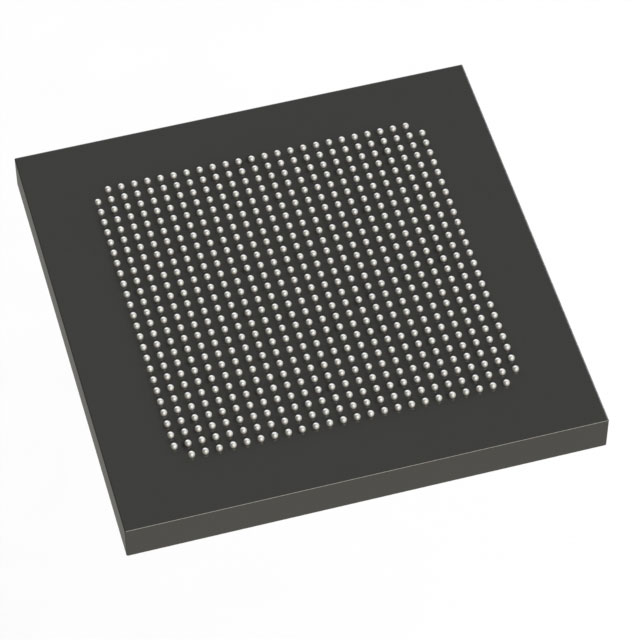
Stratix® V GS Field Programmable Gate Array (FPGA) IC 360 13312000 236000 780-BBGA, FCBGA |
|---|---|
| Quantity | 57 Available (as of June 10, 2026) |

| Product Category | Field Programmable Gate Array (FPGA) |
|---|---|
| Manufacturer | Intel |
| Manufacturing Status | Obsolete |
| Manufacturer Standard Lead Time | Contact Us |
| Datasheet |
Specifications & Environmental
| Device Package | 780-HBGA (33x33) | Grade | Industrial | Operating Temperature | -40°C – 100°C | ||
|---|---|---|---|---|---|---|---|
| Package / Case | 780-BBGA, FCBGA | Number of I/O | 360 | Voltage | 820 mV - 880 mV | ||
| Mounting Method | Surface Mount | RoHS Compliance | RoHS Compliant | REACH Compliance | REACH Unknown | ||
| Moisture Sensitivity Level | 3 (168 Hours) | Number of LABs/CLBs | 89000 | Number of Logic Elements/Cells | 236000 | ||
| Number of Gates | N/A | ECCN | 3A001A2C | HTS Code | 8542.39.0001 | ||
| Qualification | N/A | Total RAM Bits | 13312000 |
Overview of 5SGSMD3E2H29I2LN – Stratix V GS FPGA, 360 I/O, 780-BBGA
The 5SGSMD3E2H29I2LN is an Intel Stratix® V GS field-programmable gate array (FPGA) in a 780-BBGA (FCBGA) package targeted at high-performance, DSP-centric and transceiver-based applications. Built on the Stratix V family architecture, this GS variant combines a high logic count and substantial on-chip memory with integrated transceiver and DSP resources to address bandwidth- and compute-intensive designs.
Key Features
- Core & process — Stratix V family device architecture implemented in 28-nm process technology, delivering the building blocks described for the family.
- Logic capacity — Approximately 236,000 logic elements to implement large, complex FPGA designs.
- Embedded memory — Approximately 13.3 Mbits of on-chip RAM (13,312,000 total RAM bits) using the family’s 20-Kbit embedded memory blocks.
- DSP resources — GS family provides an abundance of variable-precision DSP blocks for high-performance digital signal processing workloads.
- Transceiver capability — GS devices include integrated transceivers with 14.1‑Gbps data-rate capability for high-speed serial interfaces.
- I/O and package — 360 user I/O pins in a 780-BBGA (FCBGA) supplier package 780-HBGA (33×33), surface-mount mounting type for system-level integration.
- Power — Core voltage supply operating range specified at 820 mV to 880 mV for the device.
- Temperature and grade — Industrial-grade device rated for operation from −40 °C to 100 °C.
- Integration and hard IP — Stratix V family includes Embedded HardCopy Block support and a set of integrated hard IP blocks used for IP instantiation and migration paths.
Typical Applications
- High-performance DSP systems — Use the GS variant’s dense DSP resources and embedded memory for compute-intensive signal processing and algorithm acceleration.
- Optical and backplane interfaces — Integrated transceivers with multi-gigabit capability support high-speed serial links for optical transport and backplane applications.
- Networking and packet processing — Large logic capacity and on-chip memory enable complex packet-processing pipelines and high-throughput networking functions.
- Broadcast and military communications — DSP-centric architecture and transceiver support suit modulation, encoding, and other real-time communications processing tasks.
Unique Advantages
- High logic and memory density: Approximately 236,000 logic elements and about 13.3 Mbits of embedded RAM let you map large designs on a single device, reducing board-level complexity.
- DSP-optimized resources: Variable-precision DSP blocks speed implementation of math-intensive kernels such as filtering, transforms, and complex arithmetic.
- Integrated high-speed serial I/O: 14.1‑Gbps-capable transceivers enable direct connection to high-bandwidth links without external SerDes components.
- Industrial temperature rating: −40 °C to 100 °C operation supports deployment in industrial environments requiring extended thermal range.
- System-level packaging: 780-BBGA (33×33) surface-mount package provides dense I/O and a compact footprint for space-constrained, high-performance boards.
- Family-level ecosystem: The Stratix V family architecture and Embedded HardCopy Block support simplify IP reuse and migration across development and production flows.
Why Choose 5SGSMD3E2H29I2LN?
The 5SGSMD3E2H29I2LN brings a balance of high logic count, substantial embedded memory, abundant DSP resources, and multi-gigabit transceivers in an industrial-grade Stratix V GS device. It is suited for engineers designing bandwidth- and compute-intensive systems that require a single, integrated device to minimize board complexity and accelerate time to market.
Choose this device for scalable DSP implementations, high-speed interface designs, and systems where dense logic, robust on-chip memory, and industrial temperature operation are key selection criteria.
Request a quote or submit an inquiry to learn about availability, pricing, and lead times for 5SGSMD3E2H29I2LN.


Date Founded: 1968
Headquarters: Santa Clara, California, USA
Employees: 130,000+
Revenue: $54.23 Billion
Certifications and Memberships: ISO9001:2015, ISO14001:2015, ISO17025:2017, ISO27001:2022, ISO45001:2018, ISO50001:2018


