
5SGSMD3E3H29C2L
| Part Description |
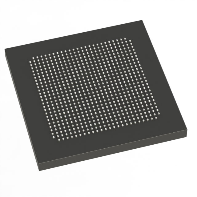
Stratix® V GS Field Programmable Gate Array (FPGA) IC 360 13312000 236000 780-BBGA, FCBGA |
|---|---|
| Quantity | 36 Available (as of June 15, 2026) |

| Product Category | Field Programmable Gate Array (FPGA) |
|---|---|
| Manufacturer | Intel |
| Manufacturing Status | Obsolete |
| Manufacturer Standard Lead Time | Contact Us |
| Datasheet |
Specifications & Environmental
| Device Package | 780-HBGA (33x33) | Grade | Commercial | Operating Temperature | 0°C – 85°C | ||
|---|---|---|---|---|---|---|---|
| Package / Case | 780-BBGA, FCBGA | Number of I/O | 360 | Voltage | 820 mV - 880 mV | ||
| Mounting Method | Surface Mount | RoHS Compliance | RoHS Compliant | REACH Compliance | REACH Unknown | ||
| Moisture Sensitivity Level | 3 (168 Hours) | Number of LABs/CLBs | 89000 | Number of Logic Elements/Cells | 236000 | ||
| Number of Gates | N/A | ECCN | 3A001A2C | HTS Code | 8542.39.0001 | ||
| Qualification | N/A | Total RAM Bits | 13312000 |
Overview of 5SGSMD3E3H29C2L – Stratix V GS FPGA, 236,000 LEs, 360 I/O, 780-BBGA
The 5SGSMD3E3H29C2L is a Stratix V GS field-programmable gate array (FPGA) offered in a 780-ball FCBGA package. Built on a 28-nm process and the Stratix V architecture, this device combines high logic density, substantial embedded memory, and DSP-targeted resources for transceiver-enabled, signal-processing applications.
With 236,000 logic elements, approximately 13.3 Mbits of on-chip RAM and 360 I/O pins, this commercial-grade device targets bandwidth- and DSP-centric systems that benefit from integrated transceivers and hardened IP options at the device-family level.
Key Features
- Logic Capacity — 236,000 logic elements to implement complex custom logic and control paths.
- Embedded Memory — Approximately 13.3 Mbits of on-chip RAM using 20-Kbit memory blocks at the device-family level for buffering and state storage.
- DSP Resources — Stratix V GS family provides abundant variable-precision DSP blocks and multiplier resources for high-performance signal processing.
- High-Speed Serial — GS devices include integrated transceivers with up to 14.1-Gbps data-rate capability (series-level feature) for backplane and optical interface applications.
- I/O Density — 360 I/O pins to support multi-channel interfaces and system integration.
- Process and Core Voltage — 28-nm TSMC technology with a device supply range of 0.820–0.880 V (core supply specified in product data).
- Package and Mounting — 780-BBGA (FCBGA) 33 × 33 supplier package in a surface-mount form factor for compact board-level integration.
- Operating Range — Commercial-grade operating temperature from 0 °C to 85 °C and RoHS compliance.
- Hard IP and Architecture — Series-level features include a redesigned adaptive logic module (ALM), multi-track routing, fractional PLLs and an Embedded HardCopy Block for hardened IP instantiation.
Typical Applications
- Telecommunications and Optical Transport — Implement packet processing, backplane interfaces and optical system functions using integrated transceivers and high logic/memory capacity.
- High-Performance DSP — Deploy variable-precision DSP blocks and large multiplier arrays for compute-intensive signal-processing pipelines.
- Network and Data Center Equipment — Use the device’s logic density and on-chip memory for traffic management, protocol offload and accelerated data-path functions.
- Broadcast and Test Equipment — Leverage transceiver capability and DSP resources for high-bandwidth streaming, capture and analysis applications.
Unique Advantages
- High logic density: 236,000 logic elements provide room for complex control, protocol and data-path implementations without external logic expansion.
- Significant on-chip memory: Approximately 13.3 Mbits of embedded RAM reduces dependence on external memory for buffering and low-latency storage.
- DSP-optimized architecture: Stratix V GS family DSP resources and multipliers support precision-tailored signal processing workflows.
- Integrated serial connectivity: Family-level transceivers with 14.1-Gbps capability enable high-bandwidth serial links for modern communications and transport interfaces.
- Compact, surface-mount package: The 780-BBGA (33 × 33) FCBGA package supports dense board-level integration while providing 360 I/O for system connectivity.
- Commercial temperature and RoHS compliance: Rated 0 °C to 85 °C and RoHS-compliant for standard commercial deployments.
Why Choose 5SGSMD3E3H29C2L?
The 5SGSMD3E3H29C2L delivers a balanced combination of logic capacity, embedded memory and DSP-oriented resources in a package designed for high-density, high-bandwidth applications. As a Stratix V GS device, it brings series-level features—like integrated transceivers and hardened IP options—together with device-specific specifications that suit communications, DSP and data-path designs.
This device is well suited for engineering teams seeking a commercial-grade FPGA with strong on-chip memory, plentiful I/O and the option to leverage Stratix V family documentation and migration paths within the vendor ecosystem.
Request a quote or submit a purchase inquiry to receive pricing, lead-time and order information for part number 5SGSMD3E3H29C2L.


Date Founded: 1968
Headquarters: Santa Clara, California, USA
Employees: 130,000+
Revenue: $54.23 Billion
Certifications and Memberships: ISO9001:2015, ISO14001:2015, ISO17025:2017, ISO27001:2022, ISO45001:2018, ISO50001:2018


