
5SGSMD3E3H29C2N
| Part Description |
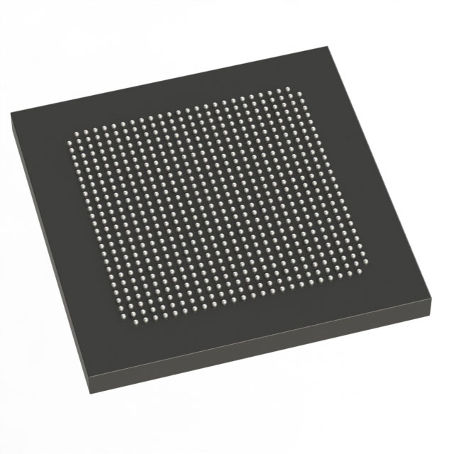
Stratix® V GS Field Programmable Gate Array (FPGA) IC 360 13312000 236000 780-BBGA, FCBGA |
|---|---|
| Quantity | 127 Available (as of June 14, 2026) |

| Product Category | Field Programmable Gate Array (FPGA) |
|---|---|
| Manufacturer | Intel |
| Manufacturing Status | Obsolete |
| Manufacturer Standard Lead Time | Contact Us |
| Datasheet |
Specifications & Environmental
| Device Package | 780-HBGA (33x33) | Grade | Commercial | Operating Temperature | 0°C – 85°C | ||
|---|---|---|---|---|---|---|---|
| Package / Case | 780-BBGA, FCBGA | Number of I/O | 360 | Voltage | 870 mV - 930 mV | ||
| Mounting Method | Surface Mount | RoHS Compliance | RoHS Compliant | REACH Compliance | REACH Unknown | ||
| Moisture Sensitivity Level | 3 (168 Hours) | Number of LABs/CLBs | 89000 | Number of Logic Elements/Cells | 236000 | ||
| Number of Gates | N/A | ECCN | 3A001A2C | HTS Code | 8542.39.0001 | ||
| Qualification | N/A | Total RAM Bits | 13312000 |
Overview of 5SGSMD3E3H29C2N – Stratix V GS FPGA, 780‑BBGA (FCBGA)
The 5SGSMD3E3H29C2N is an Intel Stratix V GS field‑programmable gate array supplied in a 780‑ball FCBGA package. It combines a high logic density fabric with abundant embedded memory and variable‑precision DSP resources tailored for transceiver‑based, DSP‑centric applications.
With 236,000 logic elements, approximately 13.3 Mbits of embedded memory and integrated transceiver capabilities described for the GS variant, this device targets bandwidth‑ and DSP‑intensive systems where programmable performance and on‑chip integration reduce system complexity.
Key Features
- Logic Capacity — 236,000 logic elements providing substantial programmable fabric for complex algorithms and control logic.
- Embedded Memory — Approximately 13.3 Mbits of on‑chip RAM implemented in 20 Kbit (M20K) blocks for high‑speed buffering and local data storage.
- Variable‑Precision DSP — GS‑class devices include an abundance of variable‑precision DSP blocks (supports up to 3,926 18×18 or 1,963 27×27 multipliers) for demanding signal processing workloads.
- Transceiver and I/O — GS devices offer integrated transceivers with 14.1 Gbps data‑rate capability and the part provides 360 I/O connections for high‑bandwidth external interfaces.
- Core Power — Low‑voltage core operation with a supply range of 870 mV to 930 mV to match system power domains.
- Package and Mounting — Surface‑mount 780‑BBGA (FCBGA) package; supplier device package 780‑HBGA (33×33) for compact board integration.
- Commercial Grade — Rated for 0°C to 85°C operating temperature and RoHS compliant for commercial applications.
- Stratix V Architecture — Built on Stratix V family architecture featuring redesigned adaptive logic modules (ALMs), comprehensive fabric clocking and fractional PLLs for flexible performance tuning.
Typical Applications
- High‑Performance DSP Systems — Leverage the large pool of variable‑precision DSP blocks and on‑chip memory for real‑time signal processing, filtering, and modulation tasks.
- Optical and Backplane Interfaces — Integrated transceiver capability and extensive I/O make the device suitable for 40G/100G‑class optical and backplane link implementations.
- Networking and Packet Processing — High logic density and embedded memory support complex packet handling, traffic management and protocol offload functions.
- Broadcast and Test Equipment — Combine DSP resources and transceivers for real‑time media processing, monitoring and test instrumentation.
Unique Advantages
- Substantial Programmable Capacity: 236,000 logic elements enable implementation of complex custom logic, accelerators and control subsystems on a single device.
- Significant On‑Chip Memory: Approximately 13.3 Mbits of embedded RAM reduces external memory dependence and improves data locality for high‑throughput designs.
- DSP‑Centric Resources: A large number of variable‑precision multipliers supports intensive signal processing tasks without offloading to external processors.
- High‑Speed I/O and Transceivers: 360 I/O pins and GS‑class transceiver capability support high‑bandwidth external interfaces and complex board‑level connectivity.
- Low‑Voltage Core: 0.87–0.93 V core supply range enables integration into modern low‑power system architectures.
- Commercial Readiness: Surface‑mount 780‑BBGA packaging and RoHS compliance simplify production and regulatory requirements for commercial products.
Why Choose 5SGSMD3E3H29C2N?
The 5SGSMD3E3H29C2N delivers a balance of programmable logic capacity, abundant embedded memory and specialized DSP resources within a compact FCBGA package—well suited for developers building transceiver‑driven, DSP‑heavy systems. Its Stratix V architecture provides flexible building blocks (ALMs, M20K memory blocks, PLLs) that speed development and enable scalable designs.
Choose this Stratix V GS device when you need on‑chip integration of logic, memory and DSP resources to reduce BOM, minimize board complexity and accelerate time‑to‑market for high‑bandwidth commercial applications.
Request a quote or submit an inquiry to obtain pricing, availability and technical support for 5SGSMD3E3H29C2N.


Date Founded: 1968
Headquarters: Santa Clara, California, USA
Employees: 130,000+
Revenue: $54.23 Billion
Certifications and Memberships: ISO9001:2015, ISO14001:2015, ISO17025:2017, ISO27001:2022, ISO45001:2018, ISO50001:2018


