
5SGSMD3E3H29C3G
| Part Description |
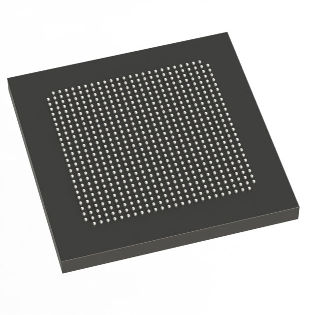
Stratix® V GS Field Programmable Gate Array (FPGA) IC 360 13312000 236000 780-BBGA, FCBGA |
|---|---|
| Quantity | 656 Available (as of June 18, 2026) |
| Product Category | Field Programmable Gate Array (FPGA) |
|---|---|
| Manufacturer | Intel |
| Manufacturing Status | Active |
| Manufacturer Standard Lead Time | 26 Weeks |
| Datasheet |
Specifications & Environmental
| Device Package | 780-HBGA (33x33) | Grade | Commercial | Operating Temperature | 0°C – 85°C | ||
|---|---|---|---|---|---|---|---|
| Package / Case | 780-BBGA, FCBGA | Number of I/O | 360 | Voltage | 820 mV - 880 mV | ||
| Mounting Method | Surface Mount | RoHS Compliance | RoHS Compliant | REACH Compliance | REACH Unaffected | ||
| Moisture Sensitivity Level | 3 (168 Hours) | Number of LABs/CLBs | 89000 | Number of Logic Elements/Cells | 236000 | ||
| Number of Gates | N/A | ECCN | N/A | HTS Code | N/A | ||
| Qualification | N/A | Total RAM Bits | 13312000 |
Overview of 5SGSMD3E3H29C3G – Stratix® V GS FPGA, 236,000 logic elements
The 5SGSMD3E3H29C3G is a Stratix® V GS field-programmable gate array (FPGA) IC in a 780-ball BGA (FCBGA) package. It integrates a large programmable fabric with substantial embedded RAM and plentiful I/O, and includes electrical and switching characteristics that cover core, periphery, and transceiver behavior.
Targeted for commercial-temperature applications, this device offers a combination of logic capacity, on-chip memory, and I/O density that supports complex digital designs where integration and predictable electrical operating conditions are required.
Key Features
- Logic Capacity 236,000 logic elements to implement large-scale programmable logic and custom digital functions.
- Logic Array Blocks Approximately 89,000 logic blocks for structured resource partitioning and design mapping.
- Embedded Memory Approximately 13.312 Mbits of embedded RAM to support buffers, FIFOs, and on-chip data storage.
- I/O Density 360 user I/O pins to support wide bus interfaces, multiple peripherals, and high-pin-count connectivity.
- Package & Mounting 780-ball BGA (FCBGA) package; supplier device package listed as 780-HBGA (33×33); surface-mount mounting type for standard PCB assembly.
- Power and Supply Range Core supply specified from 820 mV to 880 mV, enabling defined low-voltage core operation.
- Temperature and Grade Commercial grade device rated for 0 °C to 85 °C operating temperature.
- Compliance RoHS compliant.
- Electrical & Switching Characteristics Datasheet includes detailed operating-condition, power, and transceiver switching specifications for system-level integration and timing design.
Typical Applications
- High-density digital processing Large logic element count and on-chip RAM enable implementation of complex FPGA algorithms, state machines, and data-path acceleration.
- Interface aggregation 360 I/Os provide the pin count necessary for wide parallel buses, multi-channel interfaces, or mixed-signal front ends that require many external connections.
- Embedded memory buffering Approximately 13.312 Mbits of RAM supports temporary data storage, FIFOs, and buffering within throughput-heavy designs.
Unique Advantages
- Substantial logic resources: 236,000 logic elements let you consolidate multiple functions into a single FPGA, reducing board-level complexity.
- Significant embedded memory: Approximately 13.312 Mbits of on-chip RAM reduces dependence on external memory for many buffering and storage needs.
- High I/O count: 360 user I/Os enable dense peripheral and bus connectivity without additional interface chips.
- Defined low-voltage core: Core supply range of 820 mV–880 mV provides a clear electrical envelope for power-supply design and board-level integration.
- Commercial-temperature qualification: Rated for 0 °C to 85 °C operation to match requirements for commercial and many industrial-facing deployments.
- RoHS compliant: Supports lead-free assembly and global environmental requirements.
Why Choose 5SGSMD3E3H29C3G?
The 5SGSMD3E3H29C3G combines a large programmable fabric, ample embedded RAM, and a high I/O count in a 780-ball BGA package, making it suitable for complex, board-level FPGA implementations that demand integration and predictable electrical behavior. Its documented electrical and switching characteristics, including transceiver-related information in the datasheet, help engineers make informed choices for timing and power design.
This device is positioned for designers and teams developing commercial-temperature FPGA systems that require substantial on-chip resources and a compact surface-mount package. The available datasheet material supports system-level integration, verification, and power planning to aid long-term design robustness and scalability.
Request a quote or submit a pricing and availability inquiry to get lead-time and ordering information for the 5SGSMD3E3H29C3G Stratix® V GS FPGA.


Date Founded: 1968
Headquarters: Santa Clara, California, USA
Employees: 130,000+
Revenue: $54.23 Billion
Certifications and Memberships: ISO9001:2015, ISO14001:2015, ISO17025:2017, ISO27001:2022, ISO45001:2018, ISO50001:2018


