
5SGSMD3E3H29C3N
| Part Description |
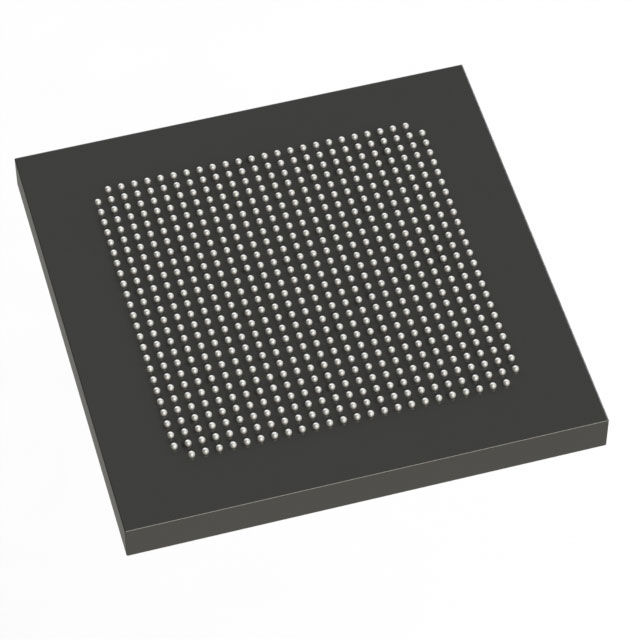
Stratix® V GS Field Programmable Gate Array (FPGA) IC 360 13312000 236000 780-BBGA, FCBGA |
|---|---|
| Quantity | 925 Available (as of June 15, 2026) |

| Product Category | Field Programmable Gate Array (FPGA) |
|---|---|
| Manufacturer | Intel |
| Manufacturing Status | Obsolete |
| Manufacturer Standard Lead Time | Contact Us |
| Datasheet |
Specifications & Environmental
| Device Package | 780-HBGA (33x33) | Grade | Commercial | Operating Temperature | 0°C – 85°C | ||
|---|---|---|---|---|---|---|---|
| Package / Case | 780-BBGA, FCBGA | Number of I/O | 360 | Voltage | 820 mV - 880 mV | ||
| Mounting Method | Surface Mount | RoHS Compliance | RoHS Compliant | REACH Compliance | REACH Unknown | ||
| Moisture Sensitivity Level | 3 (168 Hours) | Number of LABs/CLBs | 89000 | Number of Logic Elements/Cells | 236000 | ||
| Number of Gates | N/A | ECCN | 3A001A2C | HTS Code | 8542.39.0001 | ||
| Qualification | N/A | Total RAM Bits | 13312000 |
Overview of 5SGSMD3E3H29C3N – Stratix V GS FPGA, 236,000 Logic Elements, 780-BBGA FCBGA
The 5SGSMD3E3H29C3N is an Intel Stratix V GS field-programmable gate array (FPGA) in a 780-ball FCBGA package optimized for DSP-centric, transceiver-enabled designs. Built on the Stratix V family architecture, it combines a high logic capacity with substantial embedded memory and dense I/O to address high-performance signal processing, networking, and compute-accelerated applications.
This device provides a balance of logic resources, on-chip RAM, and I/O density, together with family-level features such as variable-precision DSP blocks and integrated transceiver capability, enabling high-throughput, low-latency implementations for data-intensive systems.
Key Features
- Logic Capacity — 236,000 logic elements for complex programmable logic and system integration.
- Embedded Memory — Approximately 13.3 Mbits of on-chip RAM (13,312,000 bits) to support buffering, look-up tables, and large on-chip data structures.
- DSP and FPGA Fabric (Stratix V family) — Family-level architecture includes redesigned adaptive logic modules, M20K memory blocks, and variable-precision DSP blocks suitable for high-precision signal processing.
- High-Speed Transceiver Capability (Family Feature) — Stratix V GS devices offer integrated transceivers with up to 14.1 Gbps data-rate capability for backplane and optical interface applications.
- I/O Density — 360 user I/O pins to support wide parallel interfaces and multiple high-speed links.
- Process and Core Voltage — Based on 28-nm process technology; device supply specified between 820 mV and 880 mV.
- Package — 780-ball BBGA (FCBGA) package; supplier device package listed as 780-HBGA (33×33) for compact, surface-mount board designs.
- Mounting and Grade — Surface-mount device with commercial grade operation; operating temperature range 0 °C to 85 °C.
- Compliance — RoHS compliant.
Typical Applications
- High-performance DSP systems — Use the device’s large logic array, abundant embedded memory, and family DSP blocks for real-time filtering, beamforming, and signal reconstruction.
- Networking and Packet Processing — Leverage integrated transceiver capability and dense I/O for line-rate packet processing, traffic management, and backplane interfaces.
- Optical and Serial Communications — Implement optical interface PHYs and high-speed serial protocols using the Stratix V GS transceiver features.
- Compute Acceleration — Offload algorithmic kernels to FPGA fabric using the combination of logic elements, RAM, and DSP resources for custom acceleration tasks.
Unique Advantages
- Large, integrated resource set: 236,000 logic elements and approximately 13.3 Mbits of embedded memory reduce external component count and simplify system architecture.
- Transceiver-enabled DSP focus: GS-family transceivers plus variable-precision DSP blocks enable tightly coupled serial I/O and signal processing chains.
- High I/O availability: 360 I/O pins support multi-lane interfaces, broad peripheral connectivity, and dense board-level integration.
- Compact, surface-mount package: 780-ball FCBGA (33×33) footprint provides a high pin-count solution optimized for space-constrained PCBs.
- Commercial temperature support: Rated for 0 °C to 85 °C operation for a wide range of commercial and communications equipment.
- Standards-compliant build: RoHS compliance supports modern assembly and environmental requirements.
Why Choose 5SGSMD3E3H29C3N?
The 5SGSMD3E3H29C3N positions itself as a powerful Stratix V GS-class FPGA that balances high logic capacity, substantial embedded memory, and dense I/O in a compact FCBGA package. Its family-level capabilities—such as variable-precision DSP resources and integrated transceiver support—make it well suited for designers implementing high-throughput DSP, networking, and communications systems.
This part is a fit for engineering teams needing a commercial-grade, high-resource FPGA platform that integrates logic, RAM, and I/O density to accelerate development of data- and signal-intensive designs while maintaining a compact board footprint and RoHS compliance.
Request a quote or submit a parts request to check availability, pricing, and lead-time for the 5SGSMD3E3H29C3N.


Date Founded: 1968
Headquarters: Santa Clara, California, USA
Employees: 130,000+
Revenue: $54.23 Billion
Certifications and Memberships: ISO9001:2015, ISO14001:2015, ISO17025:2017, ISO27001:2022, ISO45001:2018, ISO50001:2018


