
5SGSMD3E3H29C2LN
| Part Description |
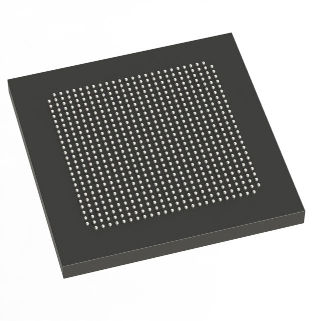
Stratix® V GS Field Programmable Gate Array (FPGA) IC 360 13312000 236000 780-BBGA, FCBGA |
|---|---|
| Quantity | 378 Available (as of June 14, 2026) |

| Product Category | Field Programmable Gate Array (FPGA) |
|---|---|
| Manufacturer | Intel |
| Manufacturing Status | Obsolete |
| Manufacturer Standard Lead Time | Contact Us |
| Datasheet |
Specifications & Environmental
| Device Package | 780-HBGA (33x33) | Grade | Commercial | Operating Temperature | 0°C – 85°C | ||
|---|---|---|---|---|---|---|---|
| Package / Case | 780-BBGA, FCBGA | Number of I/O | 360 | Voltage | 820 mV - 880 mV | ||
| Mounting Method | Surface Mount | RoHS Compliance | RoHS Compliant | REACH Compliance | REACH Unknown | ||
| Moisture Sensitivity Level | 3 (168 Hours) | Number of LABs/CLBs | 89000 | Number of Logic Elements/Cells | 236000 | ||
| Number of Gates | N/A | ECCN | 3A001A2C | HTS Code | 8542.39.0001 | ||
| Qualification | N/A | Total RAM Bits | 13312000 |
Overview of 5SGSMD3E3H29C2LN – Stratix® V GS FPGA, 236000 logic elements
The 5SGSMD3E3H29C2LN is a Stratix V GS field-programmable gate array (FPGA) in a 780-BBGA FCBGA package, designed for high-performance, DSP-centric and transceiver-based applications. Built on the Stratix V architecture, this device combines a large logic fabric with substantial on-chip memory and integrated transceivers to address bandwidth- and computation-intensive systems.
Key Features
- Process & core architecture Stratix V family architecture offering an enhanced core optimized for high-performance logic and DSP workloads.
- Logic density 236,000 logic elements for complex system integration and high gate-count designs.
- Embedded memory Approximately 13.312 Mbits of on-chip RAM (13,312,000 bits) to support large buffering, packet processing, and data-path storage.
- DSP resources GS variant devices include a rich array of variable-precision DSP blocks suitable for high-precision digital signal processing tasks.
- Integrated transceivers GS devices offer integrated transceivers with 14.1-Gbps data-rate capability for backplane and optical interface applications.
- I/O and packaging 360 I/O pins in a 780-BBGA (FCBGA) footprint; supplier device package noted as 780-HBGA (33×33). Surface-mount package simplifies board-level integration.
- Power Core supply range specified at 820 mV to 880 mV to match platform power budgeting requirements.
- Operating range & grade Commercial grade device with operating temperature from 0 °C to 85 °C and RoHS compliance.
- Embedded Hard IP Stratix V devices include an Embedded HardCopy Block for hardened IP instantiation, including PCIe Gen1/Gen2/Gen3 implementations.
Typical Applications
- High-performance DSP systems Use the abundant variable-precision DSP blocks and large logic capacity for signal processing, image processing, and compute-accelerated workloads.
- Optical and backplane communications Integrated 14.1-Gbps transceivers and high I/O count make the device suitable for backplane interfaces, optical transport, and protocol conversion.
- Networking and packet processing Large on-chip RAM and dense logic enable buffering, packet inspection, and high-throughput processing in networking equipment.
- System prototyping and ASIC path Stratix V devices provide a low-risk path to HardCopy ASICs for volume production while enabling prototyping at scale.
Unique Advantages
- High logic capacity: 236,000 logic elements let you implement complex control and data-path logic on a single device, reducing board-level complexity.
- Significant on-chip memory: Approximately 13.312 Mbits of embedded RAM supports large buffers and state storage without external memory dependencies.
- Transceiver-enabled bandwidth: Integrated 14.1-Gbps transceivers enable high-speed serial links for optical and backplane applications, simplifying PHY-level design.
- Hardened IP support: Embedded HardCopy Block accommodates hardened PCIe Gen1/Gen2/Gen3 IP instantiations to accelerate system integration.
- Compact, surface-mount package: 780-BBGA (33×33) package provides a high-pin-count solution in a compact footprint for dense system designs.
- Commercial-grade, RoHS-compliant: Designed for commercial applications with RoHS compliance for regulatory and manufacturing alignment.
Why Choose 5SGSMD3E3H29C2LN?
The 5SGSMD3E3H29C2LN positions itself as a high-density Stratix V GS FPGA suitable for DSP-intensive and transceiver-based designs that require substantial logic, embedded memory, and high-speed serial I/O. Its combination of 236,000 logic elements, approximately 13.312 Mbits of on-chip RAM, and integrated 14.1-Gbps transceivers addresses the needs of networking, communications, and high-performance compute applications.
This device is appropriate for development teams seeking a commercial-grade FPGA platform with a clear migration path to HardCopy ASICs for volume production, while benefiting from the Stratix V family’s integrated hard IP and architecture tailored for bandwidth-centric and data-intensive systems.
Request a quote or submit a request for pricing and availability to get detailed lead-time and volume information for the 5SGSMD3E3H29C2LN.


Date Founded: 1968
Headquarters: Santa Clara, California, USA
Employees: 130,000+
Revenue: $54.23 Billion
Certifications and Memberships: ISO9001:2015, ISO14001:2015, ISO17025:2017, ISO27001:2022, ISO45001:2018, ISO50001:2018


