
5SGSMD3E3H29C4N
| Part Description |
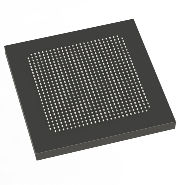
Stratix® V GS Field Programmable Gate Array (FPGA) IC 360 13312000 236000 780-BBGA, FCBGA |
|---|---|
| Quantity | 55 Available (as of June 15, 2026) |

| Product Category | Field Programmable Gate Array (FPGA) |
|---|---|
| Manufacturer | Intel |
| Manufacturing Status | Obsolete |
| Manufacturer Standard Lead Time | Contact Us |
| Datasheet |
Specifications & Environmental
| Device Package | 780-HBGA (33x33) | Grade | Commercial | Operating Temperature | 0°C – 85°C | ||
|---|---|---|---|---|---|---|---|
| Package / Case | 780-BBGA, FCBGA | Number of I/O | 360 | Voltage | 820 mV - 880 mV | ||
| Mounting Method | Surface Mount | RoHS Compliance | RoHS Compliant | REACH Compliance | REACH Unknown | ||
| Moisture Sensitivity Level | 3 (168 Hours) | Number of LABs/CLBs | 89000 | Number of Logic Elements/Cells | 236000 | ||
| Number of Gates | N/A | ECCN | 3A001A2C | HTS Code | 8542.39.0001 | ||
| Qualification | N/A | Total RAM Bits | 13312000 |
Overview of 5SGSMD3E3H29C4N – Stratix® V GS FPGA, 780-BBGA FCBGA, 360 I/O
The 5SGSMD3E3H29C4N is a Stratix V GS field programmable gate array (FPGA) in a 780-ball BGA FCBGA package. It combines a high-density logic fabric with abundant DSP resources and integrated transceiver capability targeted at transceiver-centric and DSP-intensive designs.
Designed for bandwidth- and compute-focused applications, this device delivers a mix of programmable logic, embedded memory, and high-speed I/O, with core voltage operation and commercial temperature grading suitable for mainstream embedded and network equipment.
Key Features
- Logic Capacity — 236,000 logic elements (cells) to implement complex digital designs and custom compute pipelines.
- Embedded Memory — Approximately 13.3 Mbits of on-chip RAM (13,312,000 bits) organized in M20K memory blocks for buffers, packet storage, and intermediate data processing.
- DSP Resources — Stratix V GS family supports variable-precision DSP blocks and an abundance of multipliers, enabling high-performance signal-processing implementations (family-level multiplier counts documented in device handbook).
- I/O and Transceivers — 360 I/Os and GS-class integrated transceivers with 14.1 Gbps data rate capability for backplane and optical interface applications.
- Process and Fabric — 28‑nm device architecture with redesigned adaptive logic modules (ALMs) and a comprehensive fabric clocking network as described for the Stratix V family.
- Package — 780-BBGA, FCBGA (supplier device package: 780-HBGA, 33×33 mm) for high-pin-count board designs.
- Power and Temperature — Core supply range 820 mV to 880 mV; commercial operating temperature 0°C to 85°C.
- Compliance — RoHS compliant.
- Hard IP and ASIC Path — Supports embedded hard IP blocks and a low-risk prototyping path toward HardCopy V ASICs (Stratix V family feature).
Typical Applications
- High‑performance DSP systems — Implement multi-channel filtering, FFTs, and precision arithmetic using the device’s variable-precision DSP blocks and abundant multipliers.
- Network and telecom infrastructure — Support packet processing, backplane interfaces, and optical module interfacing with 14.1 Gbps transceiver capability and large on-chip memory for buffering.
- Broadcast and video processing — Handle real-time video pipelines and format conversion with the combination of high logic capacity and sizable embedded RAM.
- High-performance computing (HPC) acceleration — Offload compute kernels and custom accelerators requiring dense logic and DSP resources.
Unique Advantages
- High logic density: 236,000 logic elements provide room for complex system-on-chip designs and deep custom logic integration.
- Embedded memory for data-intensive tasks: Approximately 13.3 Mbits of on-chip RAM reduces external memory dependence for buffering and intermediate storage.
- Transceiver-enabled connectivity: GS-class transceivers rated to 14.1 Gbps enable robust high-speed links for backplane and optical interfaces.
- DSP-optimized architecture: Variable-precision DSP blocks and family-level multiplier resources accelerate signal-processing workloads.
- Proven Stratix V platform: Architectural features such as ALMs, M20K memory blocks, and embedded hard IP blocks streamline implementation and migration toward HardCopy ASICs where applicable.
- Commercial-grade operating envelope: Core voltage and operating temperature range suitable for mainstream embedded and networking products.
Why Choose 5SGSMD3E3H29C4N?
The 5SGSMD3E3H29C4N delivers a balanced combination of high-density logic, substantial on-chip memory, DSP capability, and high-speed I/O in a 780-ball FCBGA package. It is positioned for designers building transceiver-based, DSP-intensive, and bandwidth-centric systems who require integrated memory and robust connectivity options.
Choosing this Stratix V GS device supports scalable development on a documented FPGA family with embedded hard IP and a defined prototyping path, providing long-term design flexibility and a route to hardened implementations when needed.
Request a quote or submit an inquiry for pricing and availability of the 5SGSMD3E3H29C4N to evaluate fit for your next design project.


Date Founded: 1968
Headquarters: Santa Clara, California, USA
Employees: 130,000+
Revenue: $54.23 Billion
Certifications and Memberships: ISO9001:2015, ISO14001:2015, ISO17025:2017, ISO27001:2022, ISO45001:2018, ISO50001:2018


