
5SGSMD3E3H29I3N
| Part Description |
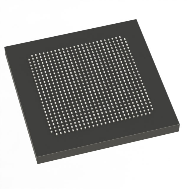
Stratix® V GS Field Programmable Gate Array (FPGA) IC 360 13312000 236000 780-BBGA, FCBGA |
|---|---|
| Quantity | 454 Available (as of June 15, 2026) |
| Product Category | Field Programmable Gate Array (FPGA) |
|---|---|
| Manufacturer | Intel |
| Manufacturing Status | Obsolete |
| Manufacturer Standard Lead Time | Contact Us |
| Datasheet |
Specifications & Environmental
| Device Package | 780-HBGA (33x33) | Grade | Industrial | Operating Temperature | -40°C – 100°C | ||
|---|---|---|---|---|---|---|---|
| Package / Case | 780-BBGA, FCBGA | Number of I/O | 360 | Voltage | 820 mV - 880 mV | ||
| Mounting Method | Surface Mount | RoHS Compliance | RoHS Compliant | REACH Compliance | REACH Unknown | ||
| Moisture Sensitivity Level | 3 (168 Hours) | Number of LABs/CLBs | 89000 | Number of Logic Elements/Cells | 236000 | ||
| Number of Gates | N/A | ECCN | 3A001A2C | HTS Code | 8542.39.0001 | ||
| Qualification | N/A | Total RAM Bits | 13312000 |
Overview of 5SGSMD3E3H29I3N – Stratix® V GS Field Programmable Gate Array (FPGA) IC, 360 I/O, approximately 13.312 Mbits RAM, 236,000 logic elements, 780-BBGA FCBGA
The 5SGSMD3E3H29I3N is a Stratix® V GS family FPGA offered in an industrial temperature grade and a high-density 780-ball BGA package. It provides a large on-chip logic resource and embedded memory capacity suitable for complex digital designs that require substantial I/O and long-term reliability in industrial environments.
With 236,000 logic elements, approximately 13.312 Mbits of embedded RAM, and up to 360 programmable I/O, this device targets designs that need significant logic density, extensive on-chip memory, and a broad I/O complement within a surface-mount FCBGA package.
Key Features
- Core Logic 236,000 logic elements to implement wide-ranging combinational and sequential logic functions.
- Embedded Memory Approximately 13.312 Mbits of on-chip RAM for buffering, packet storage, and state data.
- I/O Capability 360 general-purpose I/O pins to support dense external connectivity and multi-channel interfaces.
- Package & Mounting 780-BBGA FCBGA package; supplier device package listed as 780-HBGA (33×33). Surface-mount mounting simplifies board assembly for compact, high-density designs.
- Power Voltage supply range of 820 mV to 880 mV to meet the device’s operating requirements.
- Temperature Grade Industrial operating temperature range from −40°C to 100°C for deployments requiring extended temperature tolerance.
- Compliance RoHS compliant to meet current environmental regulations.
Typical Applications
- High-density digital processing Implement complex logic, state machines, and datapath functions leveraging 236,000 logic elements and substantial embedded RAM.
- Industrial control & automation Use in control systems that benefit from industrial temperature range (−40°C to 100°C) and extensive I/O connectivity.
- Communications and networking Deploy where many I/O channels and on-chip memory are required for buffering and protocol handling.
Unique Advantages
- High logic density: 236,000 logic elements enable consolidation of large functions onto a single device, reducing board-level complexity.
- Significant on-chip memory: Approximately 13.312 Mbits of embedded RAM supports substantial buffering and local data storage without external memory.
- Large I/O count: 360 I/O pins provide flexibility for multi-channel interfaces and parallel connectivity to peripherals and subsystems.
- Industrial-temperature operation: Rated from −40°C to 100°C for reliable operation in demanding thermal environments.
- Compact BGA packaging: 780-ball FCBGA (780-HBGA supplier package, 33×33) enables high-density PCB layouts while supporting surface-mount assembly.
- Regulatory compliance: RoHS compliance simplifies integration into products targeting regulated markets.
Why Choose 5SGSMD3E3H29I3N?
The 5SGSMD3E3H29I3N balances high logic capacity, substantial embedded memory, and broad I/O in a robust industrial-temperature FPGA package. Its combination of 236,000 logic elements, approximately 13.312 Mbits of on-chip RAM, and 360 I/O makes it suitable for engineers consolidating complex digital systems onto a single programmable device while maintaining board-area efficiency with a 780-ball BGA surface-mount package.
This device is well suited to development teams and designs that prioritize integration, on-chip memory resources, and operation across an extended temperature range, delivering a scalable platform for medium- to high-complexity FPGA implementations.
Request a quote or submit an inquiry to receive pricing and availability information for 5SGSMD3E3H29I3N. Our team will respond with lead-time and procurement options to support your project schedule.


Date Founded: 1968
Headquarters: Santa Clara, California, USA
Employees: 130,000+
Revenue: $54.23 Billion
Certifications and Memberships: ISO9001:2015, ISO14001:2015, ISO17025:2017, ISO27001:2022, ISO45001:2018, ISO50001:2018


