
5SGSMD3H3F35C2LN
| Part Description |
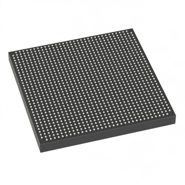
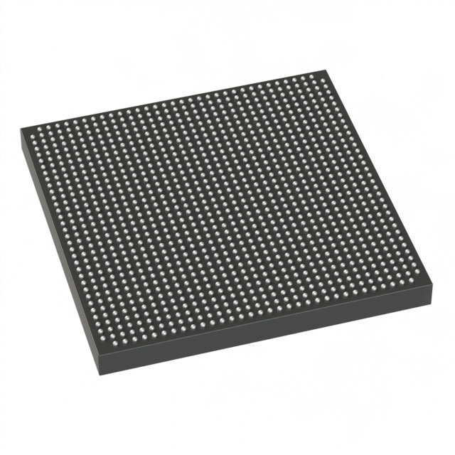
Stratix® V GS Field Programmable Gate Array (FPGA) IC 432 13312000 236000 1152-BBGA, FCBGA |
|---|---|
| Quantity | 193 Available (as of October 8, 2026) |
| Product Category | Field Programmable Gate Array (FPGA) |
|---|---|
| Manufacturer | Intel |
| Manufacturing Status | Obsolete |
| Manufacturer Standard Lead Time | Contact Us |
| Datasheet |
Specifications & Environmental
| Device Package | 1152-FBGA (35x35) | Grade | Commercial | Operating Temperature | 0°C – 85°C | ||
|---|---|---|---|---|---|---|---|
| Package / Case | 1152-BBGA, FCBGA | Number of I/O | 432 | Voltage | 820 mV - 880 mV | ||
| Mounting Method | Surface Mount | RoHS Compliance | RoHS Compliant | REACH Compliance | REACH Unknown | ||
| Moisture Sensitivity Level | 3 (168 Hours) | Number of LABs/CLBs | 89000 | Number of Logic Elements/Cells | 236000 | ||
| Number of Gates | N/A | ECCN | 3A001A2C | HTS Code | 8542.39.0001 | ||
| Qualification | N/A | Total RAM Bits | 13312000 |
Overview of 5SGSMD3H3F35C2LN – Stratix® V GS FPGA, 236,000 logic elements, 1152-BBGA
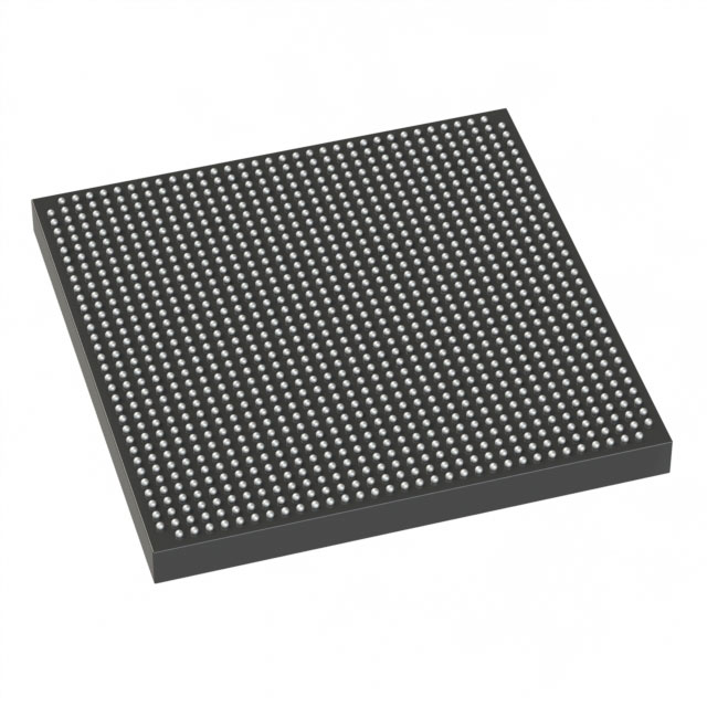
The 5SGSMD3H3F35C2LN is an Intel Stratix® V GS field-programmable gate array (FPGA) supplied in a 1152-BBGA surface-mount package. It is built on the Stratix V architecture and is targeted at DSP-centric, transceiver-enabled, and data-intensive applications.
With an enhanced core architecture, integrated hard IP blocks and high-speed transceiver capability inherent to the Stratix V family, this device delivers a balance of high logic capacity, on-chip memory, and DSP resources for demanding compute and bandwidth-centric systems.
Key Features
- Core architecture Built on the Stratix V device architecture with enhanced adaptive logic modules and a comprehensive fabric clocking network as described for the family.
- Logic capacity Provides 236,000 logic elements for complex programmable logic and control functions.
- Embedded memory Approximately 13.3 Mbits of on-chip RAM (13,312,000 bits) organized in 20 Kbit M20K memory blocks for buffering, packet storage, and intermediate data.
- DSP resources Stratix V GS devices include abundant variable-precision DSP blocks, supporting up to 3,926 18×18 or 1,963 27×27 multipliers for high-precision signal processing.
- Integrated transceivers GS devices in the Stratix V family offer integrated transceivers with 14.1-Gbps data-rate capability for backplane and optical interface applications.
- I/O and packaging 432 user I/O pins in a 1152-BBGA (supplier package: 1152-FBGA, 35×35) surface-mount package to support dense board-level connectivity.
- Power Core supply operating range specified at 820 mV to 880 mV for device power planning.
- Operating conditions & grade Commercial-grade device with an operating temperature range of 0°C to 85°C.
- Compliance RoHS compliant.
Typical Applications
- High‑performance DSP systems Leverage the variable-precision DSP blocks and large multiplier array for signal processing, filtering, and real-time compute tasks.
- Transceiver-based communications Use integrated 14.1-Gbps transceivers and abundant on-chip memory for backplane, optical interface, and packet-processing applications.
- Data‑intensive networking Support 40G/100G and other high-bandwidth data paths where logic density and memory bandwidth are required.
- Broadcast and compute acceleration Apply the device’s DSP and memory resources to video processing, encoding, and compute acceleration workloads.
- Prototype to ASIC flow Prototype designs on Stratix V GS FPGAs with the option to migrate to HardCopy V ASICs for higher-volume production.
Unique Advantages
- High programmable capacity: 236,000 logic elements provide the silicon real estate needed for complex control, protocol, and processing functions.
- Significant on-chip memory: Approximately 13.3 Mbits of embedded RAM reduce external memory dependence and lower system-level latency.
- DSP‑focused architecture: A large array of variable-precision DSP blocks and multipliers enables high-precision, high-throughput digital signal processing inside the FPGA fabric.
- Integrated high-speed I/O: 432 I/O pins plus integrated transceivers simplify board-level design for high-bandwidth interfaces.
- Production scalability: Stratix V devices support a low-risk path to HardCopy V ASICs for cost-effective migration from prototype to production.
- Commercial readiness: Surface-mount 1152-BBGA packaging and RoHS compliance streamline assembly and regulatory requirements for commercial products.
Why Choose 5SGSMD3H3F35C2LN?
The 5SGSMD3H3F35C2LN delivers a balanced combination of logic density, embedded memory, DSP horsepower, and transceiver capability within the Stratix V GS family. It is suited to engineers designing transceiver-enabled, DSP‑centric, and data-intensive systems that require on-chip compute and memory resources in a commercial-grade FPGA.
Supported by Stratix V device documentation and the documented HardCopy migration path, this device offers a practical solution for teams that need both a high-performance prototyping platform and a clear route to volume production.
Request a quote or submit an inquiry to obtain pricing, availability, and lead-time information for the 5SGSMD3H3F35C2LN.





















Date Founded: 1968
Headquarters: Santa Clara, California, USA
Employees: 130,000+
Revenue: $54.23 Billion
Certifications and Memberships: ISO9001:2015, ISO14001:2015, ISO17025:2017, ISO27001:2022, ISO45001:2018, ISO50001:2018


