
5SGSMD4H3F35C3N
| Part Description |
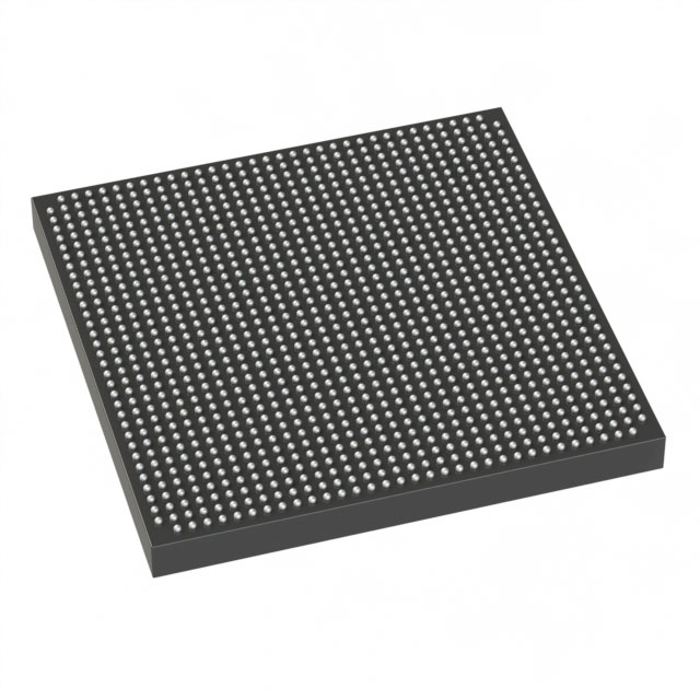
Stratix® V GS Field Programmable Gate Array (FPGA) IC 432 19456000 360000 1152-BBGA, FCBGA |
|---|---|
| Quantity | 1,011 Available (as of June 10, 2026) |

| Product Category | Field Programmable Gate Array (FPGA) |
|---|---|
| Manufacturer | Intel |
| Manufacturing Status | Obsolete |
| Manufacturer Standard Lead Time | Contact Us |
| Datasheet |
Specifications & Environmental
| Device Package | 1152-FBGA (35x35) | Grade | Commercial | Operating Temperature | 0°C – 85°C | ||
|---|---|---|---|---|---|---|---|
| Package / Case | 1152-BBGA, FCBGA | Number of I/O | 432 | Voltage | 820 mV - 880 mV | ||
| Mounting Method | Surface Mount | RoHS Compliance | RoHS Compliant | REACH Compliance | REACH Unknown | ||
| Moisture Sensitivity Level | 3 (168 Hours) | Number of LABs/CLBs | 135840 | Number of Logic Elements/Cells | 360000 | ||
| Number of Gates | N/A | ECCN | 3A001A2C | HTS Code | 8542.39.0001 | ||
| Qualification | N/A | Total RAM Bits | 19456000 |
Overview of 5SGSMD4H3F35C3N – Stratix® V GS FPGA, 1152-BBGA (35×35)
The 5SGSMD4H3F35C3N is a Stratix V GS field programmable gate array (FPGA) in a 1152-BBGA FCBGA package. It implements Intel's 28‑nm Stratix V architecture and is targeted at transceiver-driven, DSP‑centric and high‑bandwidth applications.
With approximately 360,000 logic elements, roughly 19.46 Mbits of embedded memory, and support for high‑speed transceivers and integrated hard IP blocks, this device is designed to deliver high integration for data‑intensive communications, FPGA‑based DSP processing, and optical/backplane interface applications.
Key Features
- Core architecture Stratix V family architecture implemented on a 28‑nm process with an enhanced core and Altera adaptive logic modules for high‑performance logic integration.
- Logic density Approximately 360,000 logic elements to support complex, high‑gate‑count designs.
- Embedded memory Approximately 19.46 Mbits of on‑chip RAM (M20K memory blocks) for buffering, packet processing, and DSP workflows.
- DSP and hard IP GS‑variant Stratix V devices include abundant variable‑precision DSP resources and support integrated hard IP including customizable Embedded HardCopy blocks for PCIe Gen1/Gen2/Gen3 instantiation (family‑level feature).
- Transceivers GS devices provide integrated transceivers with 14.1‑Gbps capability; the Stratix V family supports transceivers up to 28.05‑Gbps on specific variants (family‑level information).
- I/O and packaging 432 I/O pins in a 1152‑BBGA (1152‑FBGA, 35×35) supplier package for dense board integration and high pin count designs. Surface mount package.
- Power Core supply range specified at 820 mV to 880 mV to match system power budgeting and core voltage requirements.
- Operating range & compliance Commercial grade device with operating temperature 0 °C to 85 °C and RoHS compliance for regulatory conformance.
Typical Applications
- Optical and backplane communications High‑bandwidth transceiver support and on‑chip memory make this device suitable for 40G/100G class optical interfaces and backplane bridging.
- DSP‑centric systems Variable‑precision DSP resources and substantial logic density enable signal processing tasks found in broadcast, military communications, and high‑performance computing.
- Packet processing and networking Large embedded memory and high I/O count support packet buffering, traffic management, and complex networking pipelines.
- Prototype to ASIC path The Stratix V family supports a low‑risk transition path to HardCopy V ASICs (family‑level capability), useful for production scaling after FPGA prototyping.
Unique Advantages
- High logic and memory integration: Approximately 360,000 logic elements and ~19.46 Mbits of embedded memory reduce external BOM and simplify board-level memory architectures.
- Transceiver and DSP balance: Integrated transceivers and abundant DSP resources enable mixed workloads combining high‑speed I/O with intensive signal processing.
- Package options for dense designs: 1152‑BBGA (35×35) package and 432 I/O support high‑pin‑count system interfaces in a compact surface‑mount form factor.
- Family‑level hard IP and prototyping path: Embedded HardCopy block support and Stratix V family features facilitate prototyping and a defined migration path to ASIC for production scaling.
- Clear power and thermal profile: Documented core supply range (820–880 mV) and commercial temperature rating (0–85 °C) enable predictable system power and thermal design.
Why Choose 5SGSMD4H3F35C3N?
The 5SGSMD4H3F35C3N positions the Stratix V GS architecture in a high‑density, transceiver‑enabled package ideal for engineers building DSP‑intensive, high‑bandwidth systems. Its combination of substantial logic elements, multi‑Mbit embedded memory, and integrated transceiver capability supports demanding data plane and signal processing designs while simplifying board integration with a high‑pin‑count FBGA package.
For teams requiring a commercial‑grade FPGA with a clear prototyping‑to‑ASIC path within the Stratix V family and documented design elements such as core voltage and operating temperature, this device provides a verifiable platform for scaling performance and integration.
Request a quote or submit a sales inquiry to get pricing, availability, and technical support information for the 5SGSMD4H3F35C3N.


Date Founded: 1968
Headquarters: Santa Clara, California, USA
Employees: 130,000+
Revenue: $54.23 Billion
Certifications and Memberships: ISO9001:2015, ISO14001:2015, ISO17025:2017, ISO27001:2022, ISO45001:2018, ISO50001:2018


