
5SGXEA3H2F35C3N
| Part Description |
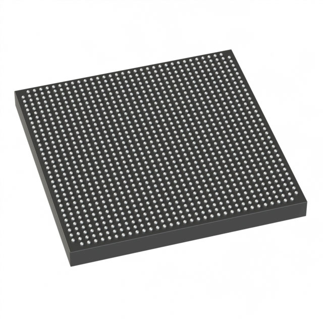
Stratix® V GX Field Programmable Gate Array (FPGA) IC 432 19456000 340000 1152-BBGA, FCBGA |
|---|---|
| Quantity | 631 Available (as of June 15, 2026) |

| Product Category | Field Programmable Gate Array (FPGA) |
|---|---|
| Manufacturer | Intel |
| Manufacturing Status | Obsolete |
| Manufacturer Standard Lead Time | Contact Us |
| Datasheet |
Specifications & Environmental
| Device Package | 1152-FBGA (35x35) | Grade | Commercial | Operating Temperature | 0°C – 85°C | ||
|---|---|---|---|---|---|---|---|
| Package / Case | 1152-BBGA, FCBGA | Number of I/O | 432 | Voltage | 820 mV - 880 mV | ||
| Mounting Method | Surface Mount | RoHS Compliance | RoHS Compliant | REACH Compliance | REACH Unknown | ||
| Moisture Sensitivity Level | 3 (168 Hours) | Number of LABs/CLBs | 128300 | Number of Logic Elements/Cells | 340000 | ||
| Number of Gates | N/A | ECCN | 3A001A2C | HTS Code | 8542.39.0001 | ||
| Qualification | N/A | Total RAM Bits | 19456000 |
Overview of 5SGXEA3H2F35C3N – Stratix® V GX FPGA, 340,000 logic elements, 432 I/O
The 5SGXEA3H2F35C3N is an Intel Stratix V GX field-programmable gate array supplied in a 1152-BBGA (1152-FBGA 35×35) surface-mount package. It provides a high-capacity programmable fabric with substantial on-chip memory and a large I/O complement for complex digital designs.
As a member of the Stratix V GX family (series datasheet), the device supports Stratix V-series capabilities including high-speed transceiver speed grades, making it suitable for designs that require dense logic, significant embedded memory, and extensive I/O resources within a commercial temperature range.
Key Features
- Core logic capacity — 340,000 logic elements (cells) to implement large-scale digital designs and parallel processing architectures.
- Embedded memory — Approximately 19.46 Mbits of on-chip RAM for large buffers, FIFOs, and local storage.
- I/O resources — 432 I/O pins to support wide interfaces and multiple high-pin-count connections.
- Transceiver family support — Part of the Stratix V GX series; series datasheet lists GX transceiver speed grade options (series-level capability up to 14.1 Gbps).
- Package and mounting — 1152-BBGA, FCBGA package; supplier device package 1152-FBGA (35×35); surface-mount for standard PCB assembly processes.
- Power supply — Core operating voltage range 820 mV to 880 mV for integration with regulated power rails.
- Temperature and grade — Commercial grade; specified operating temperature range 0 °C to 85 °C.
- Compliance — RoHS compliant.
Typical Applications
- High-speed data communications — Leverages the Stratix V GX family’s transceiver capabilities and 432 I/Os to implement multi-gigabit links and dense PHY interfaces.
- Network and packet processing — Large logic capacity and abundant embedded RAM enable packet buffering, classification, and custom network acceleration functions.
- Compute acceleration — Implements custom hardware accelerators and parallel processing pipelines using the FPGA’s 340,000 logic elements and on-chip memory.
- Prototyping and system integration — High I/O count and a standard FCBGA package make the device suitable for complex system prototypes and board-level integration.
Unique Advantages
- Highly parallel logic capacity: 340,000 logic elements provide headroom for large RTL designs and parallel architectures.
- Generous embedded memory: Approximately 19.46 Mbits of RAM reduces dependence on external memory for mid-size buffering and state storage.
- Extensive I/O connectivity: 432 I/O pins support multiple interfaces and high pin-count peripherals without additional multiplexing hardware.
- Series-level high-speed transceivers: As part of the Stratix V GX family, the device benefits from Stratix V transceiver options documented in the series datasheet.
- Compact, industry-standard package: 1152-BBGA (1152-FBGA 35×35) surface-mount package enables dense board layouts while preserving signal routing options.
- Commercial-grade reliability: Specified for 0 °C to 85 °C operation with RoHS compliance for standard commercial product environments.
Why Choose 5SGXEA3H2F35C3N?
The 5SGXEA3H2F35C3N positions itself as a high-capacity, commercially graded Stratix V GX FPGA suitable for demanding digital designs that require extensive logic, on-chip memory, and large I/O resources. Its package and power characteristics support integration into complex PCB designs while the series-level transceiver capabilities provide options for high-speed serial connectivity.
This device is appropriate for development teams and system designers building network equipment, compute accelerators, and high-throughput data-processing systems who need a verified FPGA platform within a commercial temperature range and RoHS-compliant supply chain.
Request a quote or submit a product inquiry to receive pricing, availability, and additional technical information for 5SGXEA3H2F35C3N.


Date Founded: 1968
Headquarters: Santa Clara, California, USA
Employees: 130,000+
Revenue: $54.23 Billion
Certifications and Memberships: ISO9001:2015, ISO14001:2015, ISO17025:2017, ISO27001:2022, ISO45001:2018, ISO50001:2018


