
5SGXEA3H3F35C2G
| Part Description |
Stratix® V GX Field Programmable Gate Array (FPGA) IC 432 19456000 340000 1152-BBGA, FCBGA |
|---|---|
| Quantity | 528 Available (as of June 18, 2026) |

| Product Category | Field Programmable Gate Array (FPGA) |
|---|---|
| Manufacturer | Intel |
| Manufacturing Status | Active |
| Manufacturer Standard Lead Time | 26 Weeks |
| Datasheet |
Specifications & Environmental
| Device Package | 1152-FBGA (35x35) | Grade | Commercial | Operating Temperature | 0°C – 85°C | ||
|---|---|---|---|---|---|---|---|
| Package / Case | 1152-BBGA, FCBGA | Number of I/O | 432 | Voltage | 870 mV - 930 mV | ||
| Mounting Method | Surface Mount | RoHS Compliance | RoHS Compliant | REACH Compliance | REACH Unaffected | ||
| Moisture Sensitivity Level | 3 (168 Hours) | Number of LABs/CLBs | 128300 | Number of Logic Elements/Cells | 340000 | ||
| Number of Gates | N/A | ECCN | N/A | HTS Code | N/A | ||
| Qualification | N/A | Total RAM Bits | 19456000 |
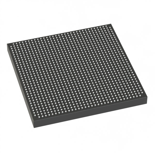
Overview of 5SGXEA3H3F35C2G – Stratix V GX FPGA, 340,000 logic elements, 1152‑BBGA
The 5SGXEA3H3F35C2G is a Stratix® V GX field programmable gate array (FPGA) from Intel designed for high-density, commercial-temperature applications. It provides a large programmable fabric, substantial on-chip memory, and a high I/O count in a 1152‑ball FCBGA package for space-efficient, surface-mount integration.
Targeted use cases include complex digital signal processing, high-throughput data-path and protocol acceleration, and multi-interface system integration where dense logic, embedded memory, and numerous I/O are required.
Key Features
- Logic Capacity Approximately 340,000 logic elements for implementing large-scale digital designs and complex algorithms.
- Embedded Memory Approximately 19.46 Mbits of on-chip RAM for buffering, packet storage, and stateful logic.
- I/O Resources 432 user I/O pins to support multiple interfaces and parallel connectivity.
- Package & Mounting 1152‑BBGA (FCBGA, 35 × 35) supplier package designed for surface-mount PCB assembly and high pin-count routing.
- Core Voltage Core voltage supply range of 870 mV to 930 mV for the device core domain.
- Temperature & Grade Commercial grade operation from 0 °C to 85 °C.
- Compliance RoHS‑compliant manufacturing status.
- Stratix V GX Family Characteristics Part of the Stratix V GX device family; the family datasheet documents commercial and industrial speed-grade and transceiver offerings for GX devices.
Typical Applications
- High‑performance networking Large logic capacity and abundant on-chip RAM enable implementation of packet processing, switching, and custom network acceleration functions.
- Signal processing and communications Stratix V GX family transceiver and fabric options make the device suitable for baseband processing, modulation/demodulation blocks, and protocol offload engines.
- Data‑path acceleration High logic density and large embedded memory support custom data-plane engines, compression, and encryption accelerators.
- Multi‑interface system controllers High I/O count supports bridging and aggregation of multiple peripheral interfaces and sensors in compact designs.
Unique Advantages
- High integration density: The combination of ~340,000 logic elements and ~19.46 Mbits of embedded RAM reduces external memory dependence and simplifies board-level design.
- Extensive I/O flexibility: 432 I/O pins provide the routing capacity needed for complex multi-interface applications without additional bridge devices.
- Compact high‑pin‑count package: The 1152‑BBGA (35 × 35) FCBGA package delivers a high pin density in a surface‑mount footprint suitable for space-constrained PCBs.
- Low‑voltage core operation: A core supply range of 870–930 mV supports low-power core operation strategies in system power budgeting.
- Commercial temperature rating: Qualified for 0 °C to 85 °C operation for standard commercial deployments.
- RoHS compliant: Manufactured to comply with RoHS directives for environmental and assembly considerations.
Why Choose 5SGXEA3H3F35C2G?
The 5SGXEA3H3F35C2G positions itself as a high-density Stratix V GX FPGA option for engineering teams needing substantial logic resources, embedded memory, and extensive I/O in a compact, surface-mount package. Its commercial-temperature rating and RoHS compliance make it suited to mainstream product applications and advanced prototypes that demand reliable on-chip resources.
Built on the Stratix V GX family platform from Intel, the device benefits from documented device characteristics and electrical specifications in the family datasheet, enabling confident integration into complex digital and data-path designs that require scalability and robust programmable resources.
If you would like pricing, availability, or to request a formal quote for 5SGXEA3H3F35C2G, submit a quote request or sales inquiry and include your required quantity and target delivery timeframe.


Date Founded: 1968
Headquarters: Santa Clara, California, USA
Employees: 130,000+
Revenue: $54.23 Billion
Certifications and Memberships: ISO9001:2015, ISO14001:2015, ISO17025:2017, ISO27001:2022, ISO45001:2018, ISO50001:2018


