
5SGXEA3K2F35C2N
| Part Description |
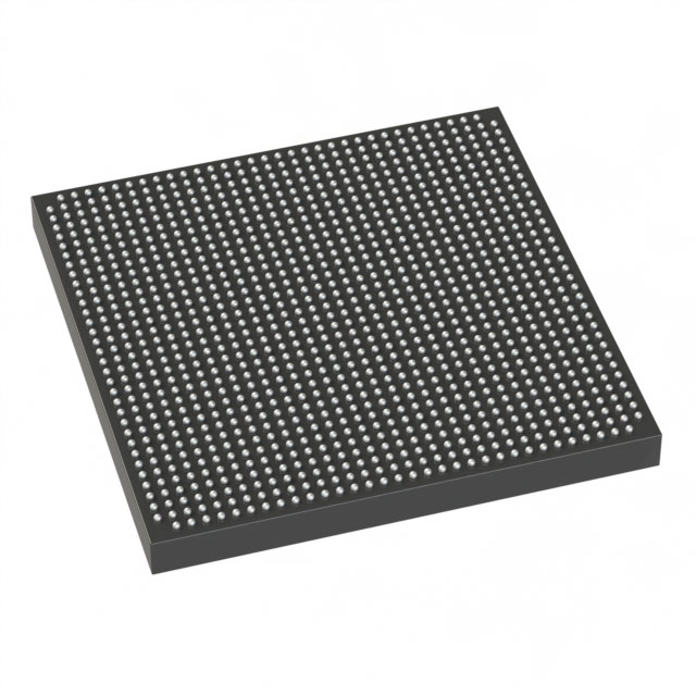
Stratix® V GX Field Programmable Gate Array (FPGA) IC 432 19456000 340000 1152-BBGA, FCBGA |
|---|---|
| Quantity | 1,252 Available (as of June 17, 2026) |
| Product Category | Field Programmable Gate Array (FPGA) |
|---|---|
| Manufacturer | Intel |
| Manufacturing Status | Obsolete |
| Manufacturer Standard Lead Time | Contact Us |
| Datasheet |
Specifications & Environmental
| Device Package | 1152-FBGA (35x35) | Grade | Commercial | Operating Temperature | 0°C – 85°C | ||
|---|---|---|---|---|---|---|---|
| Package / Case | 1152-BBGA, FCBGA | Number of I/O | 432 | Voltage | 870 mV - 930 mV | ||
| Mounting Method | Surface Mount | RoHS Compliance | RoHS Compliant | REACH Compliance | REACH Unknown | ||
| Moisture Sensitivity Level | 3 (168 Hours) | Number of LABs/CLBs | 128300 | Number of Logic Elements/Cells | 340000 | ||
| Number of Gates | N/A | ECCN | 3A001A2C | HTS Code | 8542.39.0001 | ||
| Qualification | N/A | Total RAM Bits | 19456000 |
Overview of 5SGXEA3K2F35C2N – Stratix® V GX FPGA, 340,000 logic elements, ~19.456 Mbits RAM, 432 I/Os, 1152-BBGA
The 5SGXEA3K2F35C2N is a Stratix V GX Field Programmable Gate Array (FPGA) IC offered in a 1152-BBGA FCBGA package. It delivers high on-chip logic density and embedded memory capacity for complex digital processing, signal conditioning, and I/O‑intensive designs in commercial applications.
Designed for surface-mount integration, this device combines approximately 340,000 logic elements, about 19.456 Mbits of embedded RAM, and 432 I/O pins to support large-scale programmable systems while operating within a commercial temperature range.
Key Features
- Logic Capacity Approximately 340,000 logic elements to implement large combinational and sequential logic blocks.
- Embedded Memory Approximately 19.456 Mbits of on-chip RAM for buffers, FIFOs, and application memory structures.
- I/O Density 432 I/O pins suitable for high‑pin-count interfaces and parallel bus implementations.
- Package 1152-BBGA FCBGA (supplier device package: 1152-FBGA, 35×35) optimized for board-level integration and high pin-count routing.
- Power and Voltage Specified core supply voltage range of 870 mV to 930 mV for core power budgeting and regulator selection.
- Thermal/Grade Commercial grade operation with an ambient range of 0 °C to 85 °C for a wide set of commercial environments.
- Mounting Surface-mount device for standard PCB assembly flows.
- Compliance RoHS compliant.
Typical Applications
- High-performance digital processing Large-scale logic capacity and extensive on-chip RAM make this device suitable for complex data-paths, algorithm acceleration, and custom DSP implementations.
- High-density I/O systems With 432 I/Os, the device supports multi-channel interfaces, parallel data acquisition, and dense board-level connectivity.
- Protocol bridging and interface aggregation Use the logic and memory resources to implement protocol translation, packet buffering, and aggregation functions in communication equipment.
Unique Advantages
- High logic integration: The large logic element count enables consolidation of multiple system functions into a single FPGA, reducing board-level component count.
- Substantial on‑chip memory: Approximately 19.456 Mbits of embedded RAM supports deep buffering and complex state storage without external memory.
- High I/O count: 432 I/Os provide flexibility for interfacing with multiple peripherals, sensors, and external devices simultaneously.
- Commercial temperature rating: Rated 0 °C to 85 °C for compatibility with a wide range of commercial systems and environments.
- Compact high-pin-count package: 1152-BBGA FCBGA (35×35) provides dense I/O routing while maintaining a compact PCB footprint.
- Regulated core voltage range: Defined 870–930 mV supply simplifies power-supply design and core power budgeting.
Why Choose 5SGXEA3K2F35C2N?
The 5SGXEA3K2F35C2N positions itself for designers who need a high‑capacity, I/O‑dense FPGA in a commercial-grade device. Its combination of approximately 340,000 logic elements, roughly 19.456 Mbits of embedded RAM, and 432 I/Os supports demanding digital designs that require on-chip memory and substantial interface count while fitting into a 1152‑ball BGA package.
This Stratix V GX device is suitable for development teams and system integrators seeking a scalable, high‑integration solution backed by Stratix V family documentation and engineering resources. Its power and thermal specifications aid predictable system-level power budgeting and thermal planning.
Request a quote or contact sales to discuss availability, lead times, and pricing for the 5SGXEA3K2F35C2N. Provide your BOM or project requirements to receive tailored pricing and delivery information.


Date Founded: 1968
Headquarters: Santa Clara, California, USA
Employees: 130,000+
Revenue: $54.23 Billion
Certifications and Memberships: ISO9001:2015, ISO14001:2015, ISO17025:2017, ISO27001:2022, ISO45001:2018, ISO50001:2018


