
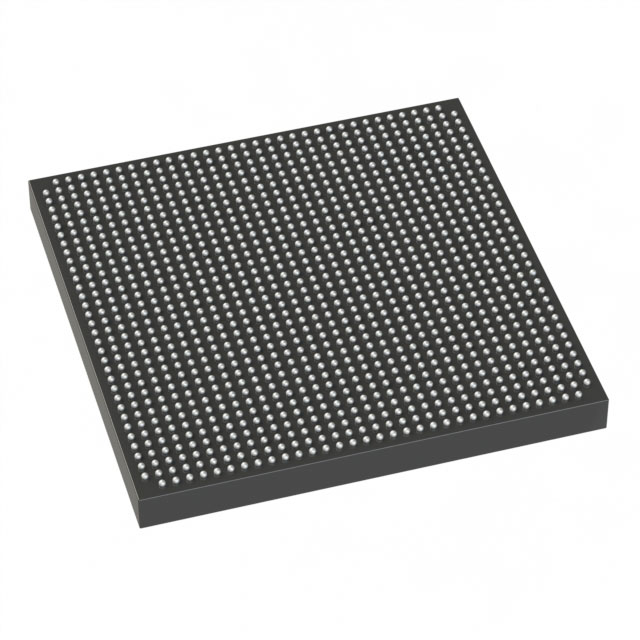
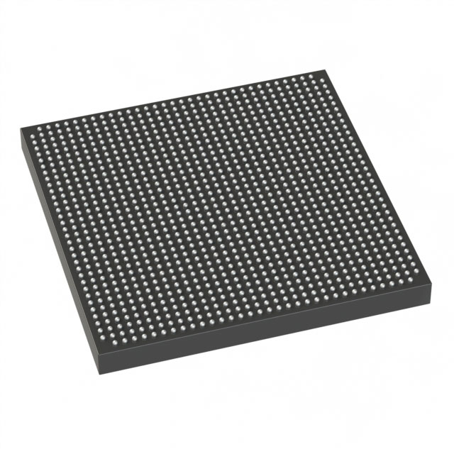
5SGXEA3K2F35C3G
| Part Description |
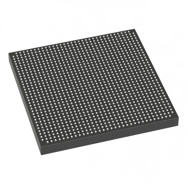
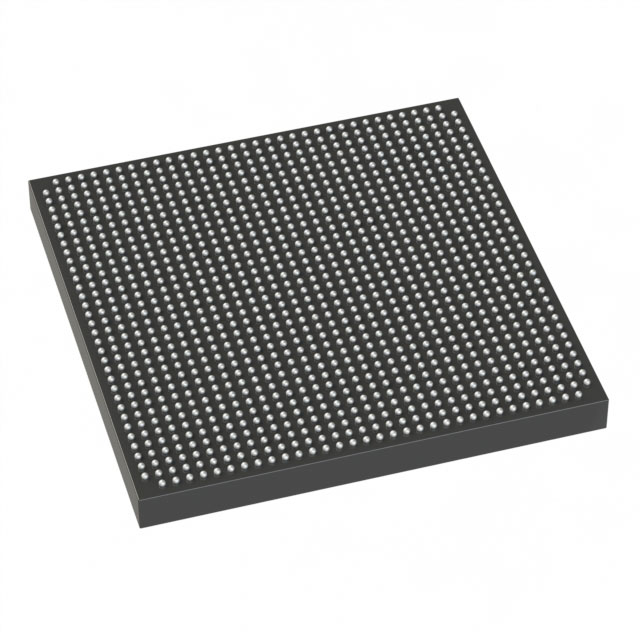
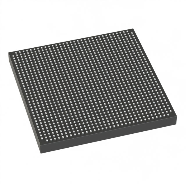
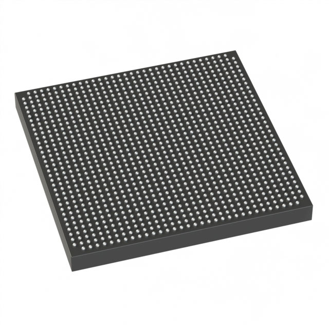
Stratix® V GX Field Programmable Gate Array (FPGA) IC 432 19456000 340000 1152-BBGA, FCBGA |
|---|---|
| Quantity | 584 Available (as of October 7, 2026) |
| Product Category | Field Programmable Gate Array (FPGA) |
|---|---|
| Manufacturer | Intel |
| Manufacturing Status | Active |
| Manufacturer Standard Lead Time | 26 Weeks |
| Datasheet |
Specifications & Environmental
| Device Package | 1152-FBGA (35x35) | Grade | Commercial | Operating Temperature | 0°C – 85°C | ||
|---|---|---|---|---|---|---|---|
| Package / Case | 1152-BBGA, FCBGA | Number of I/O | 432 | Voltage | 820 mV - 880 mV | ||
| Mounting Method | Surface Mount | RoHS Compliance | RoHS Compliant | REACH Compliance | REACH Unaffected | ||
| Moisture Sensitivity Level | 3 (168 Hours) | Number of LABs/CLBs | 128300 | Number of Logic Elements/Cells | 340000 | ||
| Number of Gates | N/A | ECCN | N/A | HTS Code | N/A | ||
| Qualification | N/A | Total RAM Bits | 19456000 |
Overview of 5SGXEA3K2F35C3G – Stratix® V GX FPGA, 340,000 logic elements, 1152‑BBGA
The 5SGXEA3K2F35C3G is a Stratix® V GX field programmable gate array (FPGA) IC from Intel, delivering high logic density and extensive on-chip memory in a 1152‑ball BGA surface‑mount package. This commercial‑grade device combines 340,000 logic elements with approximately 19.456 Mbits of embedded memory and 432 user I/O to support complex, high‑density designs.
Designed for applications that require large programmable logic resources, substantial embedded RAM, and a high I/O count, this Stratix V GX device offers a compact footprint (1152‑BBGA, FCBGA; supplier package: 1152‑FBGA, 35×35) and commercial operating specifications for mainstream embedded and digital systems.
Key Features
- Core Logic: 340,000 logic elements for implementing large-scale digital designs and custom logic accelerators.
- Embedded Memory: Approximately 19.456 Mbits of on‑chip RAM to support buffering, lookup tables, and state storage without external memory.
- I/O Capability: 432 user I/O pins to provide broad connectivity options for parallel interfaces, buses, and peripherals.
- Package & Mounting: 1152‑BBGA (FCBGA) surface‑mount package; supplier device package listed as 1152‑FBGA (35×35) for compact, board‑level integration.
- Power Supply: Core voltage supply range of 820 mV to 880 mV to match system power rails and define thermal and power budgeting.
- Commercial Grade & Temperature: Commercial temperature grade with an operating range of 0 °C to 85 °C, suitable for mainstream electronics applications.
- Compliance: RoHS‑compliant construction for environmental and regulatory alignment in commercial products.
Typical Applications
- High‑density digital processing: Implement complex logic, custom datapaths, and hardware accelerators using the device’s 340,000 logic elements and abundant on‑chip RAM.
- Multi‑interface aggregation: Use the 432 I/O pins to connect multiple parallel interfaces, expansion buses, and peripheral subsystems on a single FPGA.
- Embedded system integration: Leverage the compact 1152‑BBGA package for space‑constrained boards where high logic capacity and memory are required.
Unique Advantages
- High logic capacity: 340,000 logic elements enable consolidated implementations that reduce external logic and board complexity.
- Substantial on‑chip memory: Approximately 19.456 Mbits of embedded RAM lowers dependence on external memory components and simplifies memory architecture.
- Large I/O count: 432 I/O pins provide flexible connectivity to support parallel buses, broad sensor arrays, and multi‑lane interfaces.
- Compact package footprint: 1152‑BBGA (35×35) facilitates high‑density PCB designs while maintaining surface‑mount assembly compatibility.
- Commercial operating range: Rated for 0 °C to 85 °C to match typical conditions for commercial electronics deployments.
- RoHS compliant: Built to meet common environmental regulations for commercial products.
Why Choose 5SGXEA3K2F35C3G?
The 5SGXEA3K2F35C3G positions itself as a high‑capacity Stratix V GX FPGA option for designers needing large programmable logic resources, substantial embedded RAM, and a high I/O count in a compact BGA package. Its combination of 340,000 logic elements, approximately 19.456 Mbits of on‑chip memory, and 432 I/Os enables integration of complex digital functions while reducing external component count.
This device is well suited for teams and projects focused on high‑density digital designs and embedded systems where commercial operating conditions and RoHS compliance are required. Choosing this Stratix V GX part supports scalable designs that leverage the Intel Stratix V family characteristics and accompanying device documentation for system‑level planning.
Request a quote or submit an inquiry to receive pricing, availability, and lead‑time information for the 5SGXEA3K2F35C3G.





















Date Founded: 1968
Headquarters: Santa Clara, California, USA
Employees: 130,000+
Revenue: $54.23 Billion
Certifications and Memberships: ISO9001:2015, ISO14001:2015, ISO17025:2017, ISO27001:2022, ISO45001:2018, ISO50001:2018


