
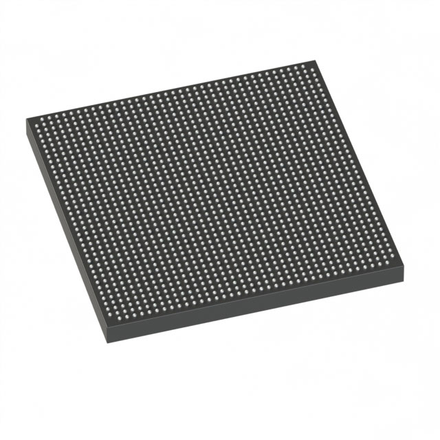
5SGXEA3K2F40I3G
| Part Description |
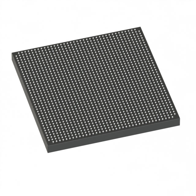
Stratix® V GX Field Programmable Gate Array (FPGA) IC 696 19456000 340000 1517-BBGA, FCBGA |
|---|---|
| Quantity | 1,046 Available (as of October 8, 2026) |
| Product Category | Field Programmable Gate Array (FPGA) |
|---|---|
| Manufacturer | Intel |
| Manufacturing Status | Active |
| Manufacturer Standard Lead Time | 26 Weeks |
| Datasheet |
Specifications & Environmental
| Device Package | 1517-FBGA (40x40) | Grade | Industrial | Operating Temperature | -40°C – 100°C | ||
|---|---|---|---|---|---|---|---|
| Package / Case | 1517-BBGA, FCBGA | Number of I/O | 696 | Voltage | 820 mV - 880 mV | ||
| Mounting Method | Surface Mount | RoHS Compliance | RoHS Compliant | REACH Compliance | REACH Unaffected | ||
| Moisture Sensitivity Level | 3 (168 Hours) | Number of LABs/CLBs | 128300 | Number of Logic Elements/Cells | 340000 | ||
| Number of Gates | N/A | ECCN | N/A | HTS Code | N/A | ||
| Qualification | N/A | Total RAM Bits | 19456000 |
Overview of 5SGXEA3K2F40I3G – Stratix® V GX Field Programmable Gate Array (FPGA), 340000 logic elements, 1517‑BBGA
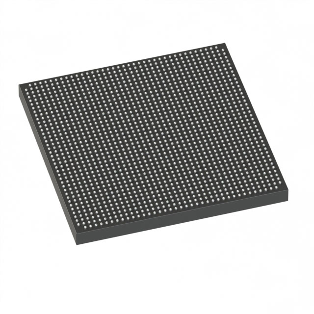
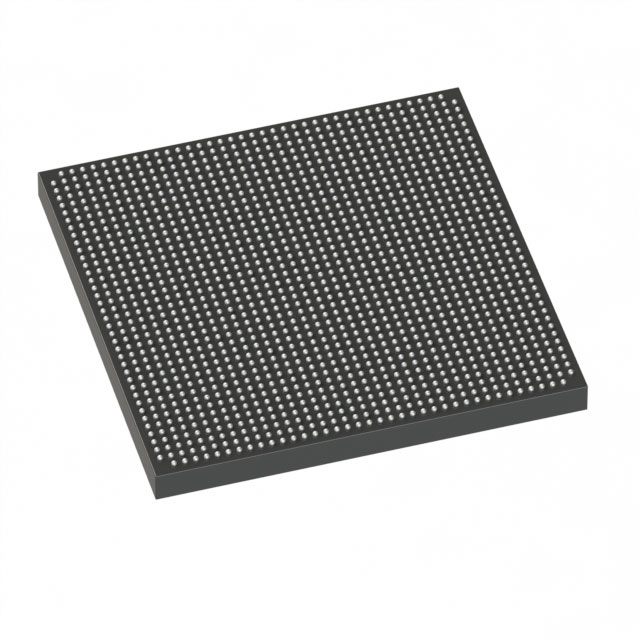
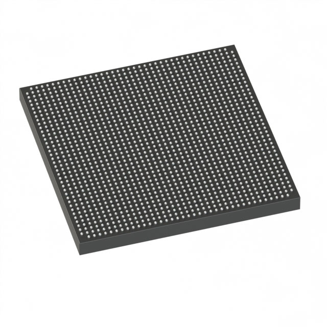
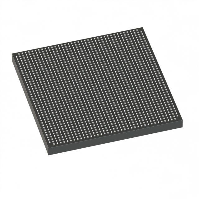
The 5SGXEA3K2F40I3G is a Stratix V GX field programmable gate array (FPGA) IC in a 1517‑BBGA (1517‑FBGA 40×40) package. It delivers a high logic capacity and abundant I/O with on‑chip embedded memory, and is offered in an industrial temperature grade.
This device targets designs that require large programmable logic resources, substantial embedded RAM, and a large number of I/O pins while operating across a wide temperature and core‑voltage range.
Key Features
- Logic Capacity — 340,000 logic elements (cell count reported in product data) to implement large, complex digital designs.
- Logic Array Blocks — 128,300 logic array blocks, providing structured building blocks for synthesis and placement.
- Embedded Memory — Approximately 19.456 Mbits of on‑chip RAM for buffering, FIFOs, and on‑device data storage.
- I/O Count — 696 I/O pins to support dense external interfaces and parallel buses.
- Power and Core Voltage — Specified core supply range of 820 mV to 880 mV for the device core voltage domain.
- Package and Mounting — 1517‑BBGA (FCBGA) package, supplier device package 1517‑FBGA (40×40); surface mount mounting type for standard PCB assembly.
- Temperature Grade — Industrial grade with operating range from –40 °C to 100 °C.
- Standards Compliance — RoHS compliant as stated in the product data.
- Family Transceiver Capability (family data) — The Stratix V GX family supports multiple transceiver speed grades across commercial and industrial offerings (family specifications described in the datasheet).
Typical Applications
- High‑density digital processing — Implement complex RTL, datapaths, and custom hardware accelerators using the device's large logic and memory resources.
- Multi‑interface bridging — Use the high I/O count to connect multiple parallel and serial interfaces in a single FPGA solution.
- Platform and subsystem integration — Consolidate multiple functions (control, protocol handling, buffering) onto one device to reduce external components.
Unique Advantages
- Extensive logic resources: 340,000 logic elements allow substantial integration of logic functions on a single device, reducing system complexity.
- Significant on‑chip memory: Approximately 19.456 Mbits of embedded RAM supports large buffering and state storage without external memory.
- High I/O density: 696 I/O pins enable broad connectivity to peripherals, sensors, and high‑pin‑count interfaces.
- Industrial temperature operation: Rated from –40 °C to 100 °C for deployment in temperature‑sensitive environments.
- Industry compliance: RoHS compliance supports environmentally preferable assembly and production processes.
- Robust packaging: 1517‑BBGA FCBGA package supports surface‑mount assembly for compact board layouts.
Why Choose 5SGXEA3K2F40I3G?
The 5SGXEA3K2F40I3G combines a high count of logic elements, substantial embedded RAM, and a large I/O complement in an industrial‑grade Stratix V GX FPGA package. It is suited for engineers and system architects who need to consolidate complex logic, memory buffering, and dense external connectivity into a single, RoHS‑compliant device while operating across a wide temperature and core‑voltage range.
Selecting this part leverages the Stratix V family’s documented electrical and transceiver capabilities (as described in the available device datasheet) and provides a scalable platform for demanding FPGA implementations.
Request a quote or submit a product inquiry to receive pricing and availability for part number 5SGXEA3K2F40I3G.





















Date Founded: 1968
Headquarters: Santa Clara, California, USA
Employees: 130,000+
Revenue: $54.23 Billion
Certifications and Memberships: ISO9001:2015, ISO14001:2015, ISO17025:2017, ISO27001:2022, ISO45001:2018, ISO50001:2018


