
5SGXEA3K2F40I3N
| Part Description |
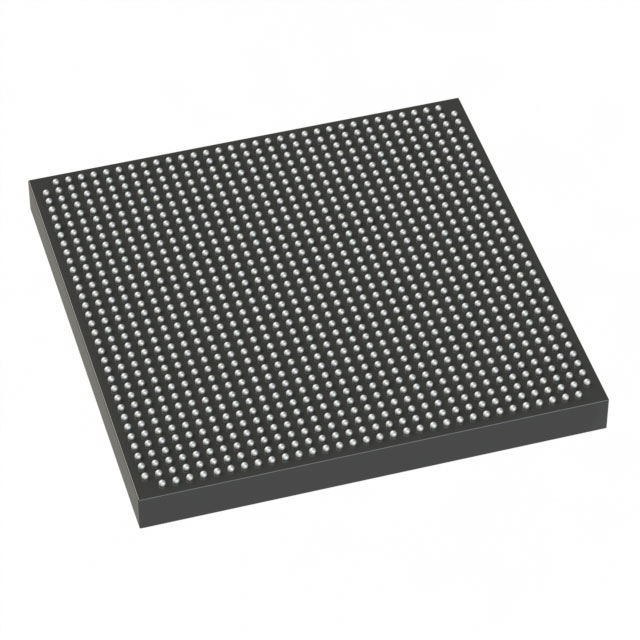
Stratix® V GX Field Programmable Gate Array (FPGA) IC 696 19456000 340000 1517-BBGA, FCBGA |
|---|---|
| Quantity | 503 Available (as of June 9, 2026) |

| Product Category | Field Programmable Gate Array (FPGA) |
|---|---|
| Manufacturer | Intel |
| Manufacturing Status | Obsolete |
| Manufacturer Standard Lead Time | Contact Us |
| Datasheet |
Specifications & Environmental
| Device Package | 1517-FBGA (40x40) | Grade | Industrial | Operating Temperature | -40°C – 100°C | ||
|---|---|---|---|---|---|---|---|
| Package / Case | 1517-BBGA, FCBGA | Number of I/O | 696 | Voltage | 820 mV - 880 mV | ||
| Mounting Method | Surface Mount | RoHS Compliance | RoHS Compliant | REACH Compliance | REACH Unknown | ||
| Moisture Sensitivity Level | 3 (168 Hours) | Number of LABs/CLBs | 128300 | Number of Logic Elements/Cells | 340000 | ||
| Number of Gates | N/A | ECCN | 3A001A2C | HTS Code | 8542.39.0001 | ||
| Qualification | N/A | Total RAM Bits | 19456000 |
Overview of 5SGXEA3K2F40I3N – Stratix® V GX FPGA, 340,000 logic elements
The 5SGXEA3K2F40I3N is a Stratix® V GX Field Programmable Gate Array (FPGA) IC from Intel. It provides a high level of on-chip integration with approximately 340,000 logic elements, approximately 19.456 Mbits of embedded memory, and 696 user I/Os, making it suitable for complex digital designs that require large logic capacity and significant I/O bandwidth.
Offered in an industrial grade device and a 1517-BBGA FCBGA package for surface-mount applications, this FPGA supports an operating voltage range of 820 mV to 880 mV and an operating temperature range of −40 °C to 100 °C.
Key Features
- Core logic capacity Approximately 340,000 logic elements enable implementation of large-scale FPGA designs and complex custom logic functions.
- Embedded memory Approximately 19.456 Mbits of on-chip RAM for buffering, lookup tables, and intermediate data storage to support data-intensive processing.
- High I/O count 696 user I/Os provide dense board-level connectivity for parallel interfaces, wide buses, and multiple peripheral connections.
- Stratix V GX transceiver capabilities Stratix V GX devices in the series are documented with transceiver speed grades up to 14.1 Gbps, offering options for high-speed serial links where required by system designs.
- Power and voltage Core supply operation specified between 820 mV and 880 mV to match platform power requirements and system power-tree design.
- Robust thermal range Industrial operating temperature from −40 °C to 100 °C supports deployment in temperature-challenging environments.
- Package and mounting 1517-BBGA (1517-FBGA, 40×40) package in a surface-mount form factor for compact board designs and high-density integration.
- Compliance RoHS compliant for environmental regulation alignment.
Typical Applications
- High-speed networking and communications Large I/O count and documented Stratix V GX transceiver speed grades support implementation of board-level network processing and multi-gigabit link functions.
- Compute acceleration and DSP Extensive logic resources and embedded RAM enable FPGA-based acceleration for compute-heavy or signal-processing workloads.
- Test, measurement and instrumentation High I/O density and broad temperature range make the device suitable for demanding instrumentation and laboratory equipment.
- Broadcast and video processing Large logic capacity and on-chip memory support real-time video pipelines and multi-channel processing tasks.
Unique Advantages
- High integration density: Approximately 340,000 logic elements and sizable embedded RAM reduce the need for external ASICs or large discrete logic counts.
- Wide connectivity: 696 I/Os provide flexibility for parallel interfaces, wide data buses, and multiple peripheral connections without immediate external multiplexing.
- Industrial-grade thermal range: Rated from −40 °C to 100 °C for reliable operation in harsh or temperature-variable environments.
- Documented transceiver performance: Stratix V GX series transceiver speed grades are defined in the device datasheet, enabling planning for multi-gigabit serial links when applicable.
- Surface-mount, high-density package: 1517-BBGA (40×40) package supports compact board layouts and high-pin-count designs.
- Regulatory alignment: RoHS compliance supports environmentally regulated product development and deployment.
Why Choose 5SGXEA3K2F40I3N?
The 5SGXEA3K2F40I3N positions itself as a high-capacity, industrial-grade Stratix V GX FPGA suited for engineers building complex, I/O-intensive systems that require substantial on-chip logic and memory. Its combination of approximately 340,000 logic elements, roughly 19.456 Mbits of embedded RAM, and 696 I/Os makes it well suited to applications in networking, compute acceleration, and real-time processing where board-level integration and thermal robustness matter.
Design teams can leverage the Stratix V series electrical and switching characteristics documented in the device datasheet to align system-level power, timing, and transceiver requirements with their project goals.
Request a quote or submit an inquiry to obtain pricing, lead time, and availability details for the 5SGXEA3K2F40I3N FPGA.


Date Founded: 1968
Headquarters: Santa Clara, California, USA
Employees: 130,000+
Revenue: $54.23 Billion
Certifications and Memberships: ISO9001:2015, ISO14001:2015, ISO17025:2017, ISO27001:2022, ISO45001:2018, ISO50001:2018


