
5SGXEA3K3F35C2LG
| Part Description |
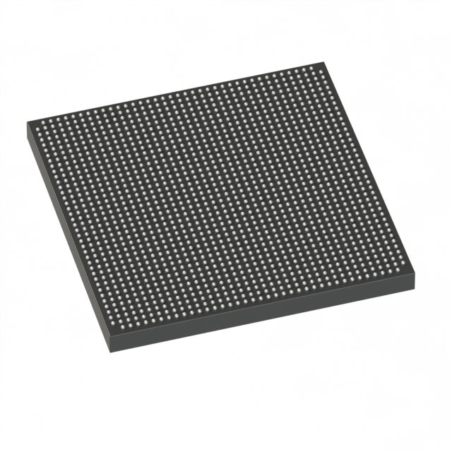
Stratix® V GX Field Programmable Gate Array (FPGA) IC 432 19456000 340000 1152-BBGA, FCBGA |
|---|---|
| Quantity | 1,211 Available (as of June 14, 2026) |

| Product Category | Field Programmable Gate Array (FPGA) |
|---|---|
| Manufacturer | Intel |
| Manufacturing Status | Active |
| Manufacturer Standard Lead Time | 26 Weeks |
| Datasheet |
Specifications & Environmental
| Device Package | 1152-FBGA (35x35) | Grade | Commercial | Operating Temperature | 0°C – 85°C | ||
|---|---|---|---|---|---|---|---|
| Package / Case | 1152-BBGA, FCBGA | Number of I/O | 432 | Voltage | 820 mV - 880 mV | ||
| Mounting Method | Surface Mount | RoHS Compliance | RoHS Compliant | REACH Compliance | REACH Unaffected | ||
| Moisture Sensitivity Level | 3 (168 Hours) | Number of LABs/CLBs | 128300 | Number of Logic Elements/Cells | 340000 | ||
| Number of Gates | N/A | ECCN | N/A | HTS Code | N/A | ||
| Qualification | N/A | Total RAM Bits | 19456000 |
Overview of 5SGXEA3K3F35C2LG – Stratix® V GX Field Programmable Gate Array (FPGA)
The 5SGXEA3K3F35C2LG is a Stratix® V GX field programmable gate array (FPGA) offering high digital logic density and on-chip memory for complex system designs. It provides 340,000 logic elements and approximately 19.46 Mbits of embedded memory, making it suitable for designs that require substantial programmable logic and internal RAM.
This commercial-grade device features 432 user I/O pins, a 1152‑FBGA (35×35) package, an internal core voltage range of 820 mV to 880 mV, and an operating temperature range of 0 °C to 85 °C. The Stratix V GX family datasheet documents transceiver and I/O timing characteristics for designs that require high-speed serial interfaces.
Key Features
- Core Logic 340,000 logic elements for large-scale programmable logic implementations.
- Embedded Memory Approximately 19.46 Mbits of total on-chip RAM bits for buffering, lookup tables, and intermediate storage.
- I/O and Package 432 user I/Os in a 1152-FBGA (35×35) FCBGA package (1152-BBGA, FCBGA), optimized for high-density board integration and surface-mount assembly.
- Transceiver Capability (Device Family) Stratix V GX devices include transceiver specifications and speed grades in the device datasheet (examples in the family reach up to 14.1 Gbps for GX channels).
- Power and Core Voltage Core supply voltage range of 820 mV to 880 mV to meet platform power requirements.
- Operating Grade Commercial temperature grade with an operating range of 0 °C to 85 °C.
- Mounting and Compliance Surface-mount device; RoHS compliant.
Typical Applications
- High-speed communications Used where Stratix V GX transceiver speed grades and plentiful I/O are needed for multi-gigabit serial links and protocol bridging.
- Networking and packet processing Large logic capacity and embedded RAM make this FPGA suitable for packet processing, switching, and network acceleration functions.
- High-performance signal processing Dense logic and on-chip memory allow implementation of DSP pipelines, video processing, and high-throughput data paths.
- Complex system integration Suitable for designs that consolidate multiple functions into a single programmable device thanks to its logic density and I/O resources.
Unique Advantages
- High logic density: 340,000 logic elements enable implementation of complex state machines, datapaths, and multi-function systems on one device.
- Substantial on-chip memory: Approximately 19.46 Mbits of embedded RAM reduces dependence on external memory for many buffering and table lookup needs.
- Robust I/O and packaging: 432 I/Os in a 1152‑FBGA (35×35) FCBGA package provide a balance of signal density and board-level routing options.
- Commercial operating range: Rated for 0 °C to 85 °C for applications targeting commercial environments.
- Low-voltage core operation: 820 mV to 880 mV core supply supports power-constrained designs and platform integration.
- RoHS compliant: Meets environmental regulations for lead-free assembly and related manufacturing requirements.
Why Choose 5SGXEA3K3F35C2LG?
The 5SGXEA3K3F35C2LG combines high logic capacity, substantial embedded memory, and extensive I/O in a commercial-grade Stratix V GX FPGA package. Its specification set is aimed at engineers developing high-performance communications, networking, and signal processing systems that require large programmable resources and on-chip RAM.
Designed for integration into surface-mount assemblies with a compact 1152-FBGA (35×35) footprint and RoHS compliance, this device is suited to teams needing a scalable, high-density FPGA platform backed by the Stratix V family datasheet and device documentation.
Request a quote or submit an inquiry for pricing, availability, and technical assistance to evaluate the 5SGXEA3K3F35C2LG for your next design.


Date Founded: 1968
Headquarters: Santa Clara, California, USA
Employees: 130,000+
Revenue: $54.23 Billion
Certifications and Memberships: ISO9001:2015, ISO14001:2015, ISO17025:2017, ISO27001:2022, ISO45001:2018, ISO50001:2018


