
5SGXEA3K2F40I2LN
| Part Description |
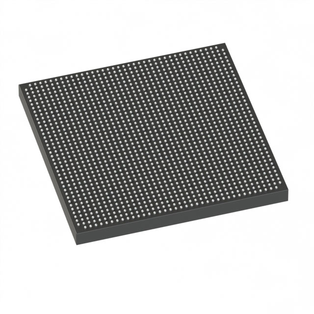
Stratix® V GX Field Programmable Gate Array (FPGA) IC 696 19456000 340000 1517-BBGA, FCBGA |
|---|---|
| Quantity | 1,240 Available (as of June 15, 2026) |

| Product Category | Field Programmable Gate Array (FPGA) |
|---|---|
| Manufacturer | Intel |
| Manufacturing Status | Obsolete |
| Manufacturer Standard Lead Time | Contact Us |
| Datasheet |
Specifications & Environmental
| Device Package | 1517-FBGA (40x40) | Grade | Industrial | Operating Temperature | -40°C – 100°C | ||
|---|---|---|---|---|---|---|---|
| Package / Case | 1517-BBGA, FCBGA | Number of I/O | 696 | Voltage | 820 mV - 880 mV | ||
| Mounting Method | Surface Mount | RoHS Compliance | RoHS Compliant | REACH Compliance | REACH Unknown | ||
| Moisture Sensitivity Level | 3 (168 Hours) | Number of LABs/CLBs | 128300 | Number of Logic Elements/Cells | 340000 | ||
| Number of Gates | N/A | ECCN | 3A001A2C | HTS Code | 8542.39.0001 | ||
| Qualification | N/A | Total RAM Bits | 19456000 |
Overview of 5SGXEA3K2F40I2LN – Stratix® V GX FPGA, 340,000 logic elements
The 5SGXEA3K2F40I2LN is a Stratix® V GX field programmable gate array (FPGA) from Intel, offered in an industrial temperature grade and supplied in a 1517-BBGA FCBGA package. It provides high logic density, substantial embedded memory, and a large I/O count for complex programmable-logic designs.
This device targets designs requiring large-scale programmable logic, significant on-chip RAM, and extensive I/O connectivity while operating across an industrial temperature range. Electrical and switching characteristics for the Stratix V family, including transceiver speed-grade information, are described in the device datasheet.
Key Features
- Core & Logic Capacity Approximately 340,000 logic elements distributed across 128,300 LABs (logic array blocks), enabling high-density programmable logic implementation.
- Embedded Memory Approximately 19.456 Mbits of on-chip RAM for buffering, LUT memory and packet/data storage.
- I/O Density Up to 696 I/O pins to support complex board-level interfacing and parallel connectivity.
- High-Speed Transceivers Stratix V GX family devices include GX transceiver speed grades; datasheet tables list GX channel options up to 14.1 Gbps for high-speed serial links.
- Power and Core Voltage Core voltage supply range from 820 mV to 880 mV to match device power requirements.
- Package & Mounting Supplied in a 1517-BBGA (1517-FBGA, 40 × 40) footprint with surface-mount mounting for compact board integration.
- Temperature & Grade Industrial grade with an operating temperature range of -40 °C to 100 °C for deployment in demanding environments.
- Compliance RoHS compliant.
Typical Applications
- High-density programmable logic Implements complex digital functions and custom hardware accelerators using the device’s large logic element and LAB count.
- Data buffering and on-chip storage Uses approximately 19.456 Mbits of embedded RAM for packet buffering, FIFOs, and intermediate data storage.
- High-speed serial interfaces Leverages the Stratix V GX transceiver speed grades for designs that require multi-gigabit serial connectivity.
- Large I/O systems Utilizes up to 696 I/Os to connect to parallel buses, peripherals, and board-level interfaces.
Unique Advantages
- High logic density: The device’s ~340,000 logic elements and 128,300 LAB count support large-scale logic integration on a single chip, reducing system-level component count.
- Significant on-chip memory: Approximately 19.456 Mbits of embedded RAM provides local storage for buffering and state retention without external memory in many use cases.
- Extensive I/O availability: 696 I/Os enable flexible board-level connectivity and support for multiple parallel interfaces simultaneously.
- Multi-gigabit serial capability: GX transceiver speed grades listed in the Stratix V documentation support high-speed serial links for communications and data transport.
- Industrial temperature range: Rated from -40 °C to 100 °C for reliable operation in industrial environments.
- Low-voltage core operation: Core supply range of 820 mV–880 mV aligns with the device’s power architecture for contemporary FPGA deployments.
Why Choose 5SGXEA3K2F40I2LN?
The 5SGXEA3K2F40I2LN offers a combination of very large programmable logic resources, substantial embedded memory, and a high I/O count in an industrial-grade Stratix V GX device package. Its specification set is suitable for complex, high-density FPGA designs that require both significant on-chip storage and extensive connectivity.
Manufactured under the Stratix V family, this device benefits from the documented electrical and switching characteristics provided in the Stratix V datasheet, enabling informed design decisions for performance, power, and thermal considerations.
Request a quote or submit an inquiry to receive pricing and availability for the 5SGXEA3K2F40I2LN. Provide your requirements and quantity to get a tailored response.


Date Founded: 1968
Headquarters: Santa Clara, California, USA
Employees: 130,000+
Revenue: $54.23 Billion
Certifications and Memberships: ISO9001:2015, ISO14001:2015, ISO17025:2017, ISO27001:2022, ISO45001:2018, ISO50001:2018


