
5SGXEA3K2F40I2LG
| Part Description |
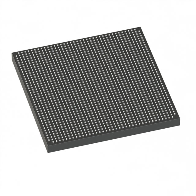
Stratix® V GX Field Programmable Gate Array (FPGA) IC 696 19456000 340000 1517-BBGA, FCBGA |
|---|---|
| Quantity | 457 Available (as of June 15, 2026) |

| Product Category | Field Programmable Gate Array (FPGA) |
|---|---|
| Manufacturer | Intel |
| Manufacturing Status | Active |
| Manufacturer Standard Lead Time | 26 Weeks |
| Datasheet |
Specifications & Environmental
| Device Package | 1517-FBGA (40x40) | Grade | Industrial | Operating Temperature | -40°C – 100°C | ||
|---|---|---|---|---|---|---|---|
| Package / Case | 1517-BBGA, FCBGA | Number of I/O | 696 | Voltage | 820 mV - 880 mV | ||
| Mounting Method | Surface Mount | RoHS Compliance | RoHS Compliant | REACH Compliance | REACH Unaffected | ||
| Moisture Sensitivity Level | 3 (168 Hours) | Number of LABs/CLBs | 128300 | Number of Logic Elements/Cells | 340000 | ||
| Number of Gates | N/A | ECCN | N/A | HTS Code | N/A | ||
| Qualification | N/A | Total RAM Bits | 19456000 |
Overview of 5SGXEA3K2F40I2LG – Stratix® V GX FPGA, 340,000 logic elements, 1517-BBGA FCBGA
The 5SGXEA3K2F40I2LG is a Stratix® V GX field-programmable gate array (FPGA) IC offering high logic density and extensive I/O in a FCBGA package. Built on the Stratix V GX family architecture, this industrial-grade device targets designs that require large on-chip memory, abundant I/O, and a high count of programmable logic resources.
Key value comes from its 340,000 logic elements, approximately 19.5 Mbits of embedded memory, and 696 I/Os, combined with an industrial operating range and a low-voltage core supply to support demanding embedded and system-level applications.
Key Features
- Logic Density 340,000 logic elements provide substantial programmable resources for complex digital designs and large-scale integration.
- Embedded Memory Approximately 19.5 Mbits of on-chip RAM to support buffering, FIFOs, and local data storage without external memory dependency.
- I/O Capability 696 user I/Os enable extensive peripheral interfacing, parallel buses, and multi-channel system connectivity.
- Low-Voltage Core Rated core voltage supply from 820 mV to 880 mV, suitable for systems optimized for low-voltage FPGA cores.
- Package 1517-BBGA (FCBGA) supplier package (1517-FBGA, 40×40) supports high-pin-count board designs and dense routing.
- Industrial Grade & Temperature Range Specified as Industrial grade with an operating temperature range of –40 °C to 100 °C for deployment in harsh environments.
- Regulatory RoHS-compliant construction for alignment with environmental and manufacturing requirements.
Typical Applications
- High-performance networking Use as a programmable logic engine for packet processing, protocol offload, and custom network functions where dense logic and many I/Os are required.
- Data center and compute acceleration Deploy as application-specific accelerators that leverage large on-chip memory and high logic capacity for algorithmic processing and data buffering.
- Industrial control and automation Implement complex control logic, real-time signal handling, and extensive sensor/actuator interfaces within the industrial temperature window.
- Signal processing Ideal for FPGA-based DSP pipelines that need sizable embedded RAM and abundant logic fabric for parallel computation.
Unique Advantages
- High integration density: 340,000 logic elements reduce the need for multiple devices, simplifying board-level design and lowering BOM complexity.
- Substantial on-chip memory: Approximately 19.5 Mbits of embedded RAM supports large local buffers and reduces external memory traffic for latency-sensitive designs.
- Extensive I/O count: 696 I/Os allow flexible interfacing options across high-pin-count systems, enabling multiple concurrent interfaces without multiplexing compromises.
- Industrial robustness: Rated for –40 °C to 100 °C operation to meet demanding environmental requirements in industrial deployments.
- Compact, high-pin package: 1517-BBGA (FCBGA) package delivers the pin density required for complex signals while maintaining a compact board footprint.
- Compliance-ready: RoHS compliance supports environmentally conscious manufacturing and regulatory alignment.
Why Choose 5SGXEA3K2F40I2LG?
The 5SGXEA3K2F40I2LG provides a combination of high logic capacity, significant embedded memory, and broad I/O in an industrial-grade Stratix V GX FPGA. It is well suited for engineers building complex, high-throughput systems that require on-chip resources to minimize external components and improve system integration.
With a low-voltage core supply and a robust temperature rating, this device supports designs that demand both performance and environmental resilience. Choose this FPGA for designs that need scalable logic resources, ample embedded RAM, and high I/O density in a compact FCBGA package.
Request a quote or submit an inquiry today to confirm availability, pricing, and lead-time for the 5SGXEA3K2F40I2LG.


Date Founded: 1968
Headquarters: Santa Clara, California, USA
Employees: 130,000+
Revenue: $54.23 Billion
Certifications and Memberships: ISO9001:2015, ISO14001:2015, ISO17025:2017, ISO27001:2022, ISO45001:2018, ISO50001:2018


