
5SGXEA4H3F35C3N
| Part Description |
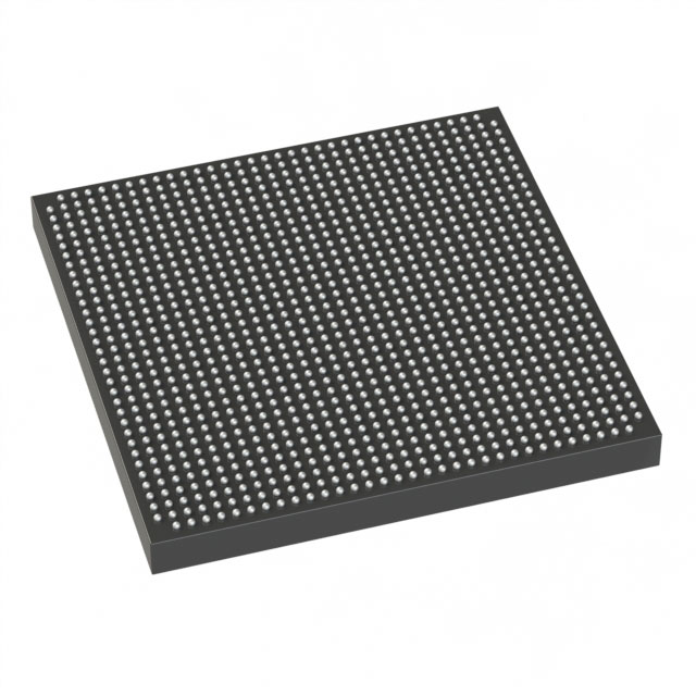
Stratix® V GX Field Programmable Gate Array (FPGA) IC 552 37888000 420000 1152-BBGA, FCBGA |
|---|---|
| Quantity | 516 Available (as of June 14, 2026) |

| Product Category | Field Programmable Gate Array (FPGA) |
|---|---|
| Manufacturer | Intel |
| Manufacturing Status | Obsolete |
| Manufacturer Standard Lead Time | Contact Us |
| Datasheet |
Specifications & Environmental
| Device Package | 1152-FBGA (35x35) | Grade | Commercial | Operating Temperature | 0°C – 85°C | ||
|---|---|---|---|---|---|---|---|
| Package / Case | 1152-BBGA, FCBGA | Number of I/O | 552 | Voltage | 820 mV - 880 mV | ||
| Mounting Method | Surface Mount | RoHS Compliance | RoHS Compliant | REACH Compliance | REACH Unknown | ||
| Moisture Sensitivity Level | 3 (168 Hours) | Number of LABs/CLBs | 158500 | Number of Logic Elements/Cells | 420000 | ||
| Number of Gates | N/A | ECCN | 3A001A2C | HTS Code | 8542.39.0001 | ||
| Qualification | N/A | Total RAM Bits | 37888000 |
Overview of 5SGXEA4H3F35C3N – Stratix® V GX FPGA, 420,000 logic elements, 1152-BBGA
The 5SGXEA4H3F35C3N is a Stratix V GX field programmable gate array (FPGA) IC in a 1152‑BBGA package designed for commercial-grade designs. It provides a large logic fabric with 420,000 logic elements and approximately 38 Mbits of embedded memory to support complex, high‑capacity FPGA implementations.
As a Stratix V GX device family member, the device is described in the Stratix V device datasheet and supports the GX transceiver speed grade options documented for the family. This package and I/O complement (552 I/Os) target dense board-level integration where high pin‑count, significant on‑chip memory, and large logic capacity are required.
Key Features
- Logic Capacity – 420,000 logic elements (cells) to implement large-scale programmable logic and complex state machines.
- Embedded Memory – Approximately 38 Mbits of total on‑chip RAM to support deep buffering, FIFOs, and large data structures.
- I/O Density – 552 user I/Os for extensive external interfacing and parallel connectivity on high‑pin‑count designs.
- Transceiver Capability (Family) – Stratix V GX devices are offered with GX transceiver speed grades as documented in the Stratix V device datasheet, enabling high‑speed serial I/O options for the family.
- Power Supply – Core voltage range specified at 820 mV to 880 mV to match system power rails and enable predictable power budgeting.
- Package and Mounting – 1152‑BBGA (FCBGA) / 1152‑FBGA (35×35) supplier package for surface‑mount assembly and compact footprint.
- Commercial Temperature Grade – Rated for operation from 0 °C to 85 °C for commercial applications.
- RoHS Compliant – Conforms to RoHS requirements for lead‑free assembly and regulatory compliance.
Typical Applications
- Complex digital and compute acceleration – Implement large custom datapaths and parallel processing using the device’s 420,000 logic elements and extensive on‑chip RAM.
- High‑pin‑count I/O systems – Boards requiring hundreds of external signals leverage the 552 I/Os for broad peripheral and bus connectivity.
- FPGA prototyping and system validation – Use the large logic and memory resources for hardware prototypes that emulate substantial ASIC or SoC functions.
- High‑speed serial interfaces (family capability) – Designs benefiting from Stratix V GX transceiver options per the device family datasheet can integrate serial links alongside dense logic.
Unique Advantages
- Large programmable fabric: 420,000 logic elements provide the capacity to consolidate complex subsystems into a single FPGA, reducing board-level component count.
- Significant on‑chip memory: Approximately 38 Mbits of embedded RAM enables local buffering and state storage without relying on external memory.
- High I/O count: 552 I/Os accommodate wide parallel buses, multiple peripherals, and extensive board-level connectivity.
- Compact, serviceable package: 1152‑BBGA (35×35) packaging offers a high pin density in a single surface‑mount package for space-constrained layouts.
- Commercial temperature rating: Guaranteed operation across 0 °C to 85 °C to meet standard commercial deployment requirements.
- Standards compliance: RoHS compliance supports lead‑free manufacturing and global environmental requirements.
Why Choose 5SGXEA4H3F35C3N?
The 5SGXEA4H3F35C3N delivers a large, commercially rated Stratix V GX FPGA option that combines very high logic density, substantial embedded memory, and a high I/O count in a 1152‑BBGA package. Its defined core voltage range and temperature rating make it suitable for commercial systems that require predictable power and thermal planning.
Engineers building complex FPGA designs, system prototypes, or high‑pin‑count boards will find this device suited to consolidate functionality, reduce external components, and support demanding on‑chip memory needs while leveraging the Stratix V family’s transceiver capabilities as documented in the device datasheet.
If you need pricing, availability, or a formal quote for 5SGXEA4H3F35C3N, request a quote or submit an inquiry to receive detailed ordering and delivery information.


Date Founded: 1968
Headquarters: Santa Clara, California, USA
Employees: 130,000+
Revenue: $54.23 Billion
Certifications and Memberships: ISO9001:2015, ISO14001:2015, ISO17025:2017, ISO27001:2022, ISO45001:2018, ISO50001:2018


