
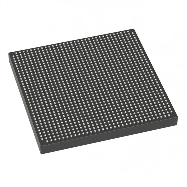
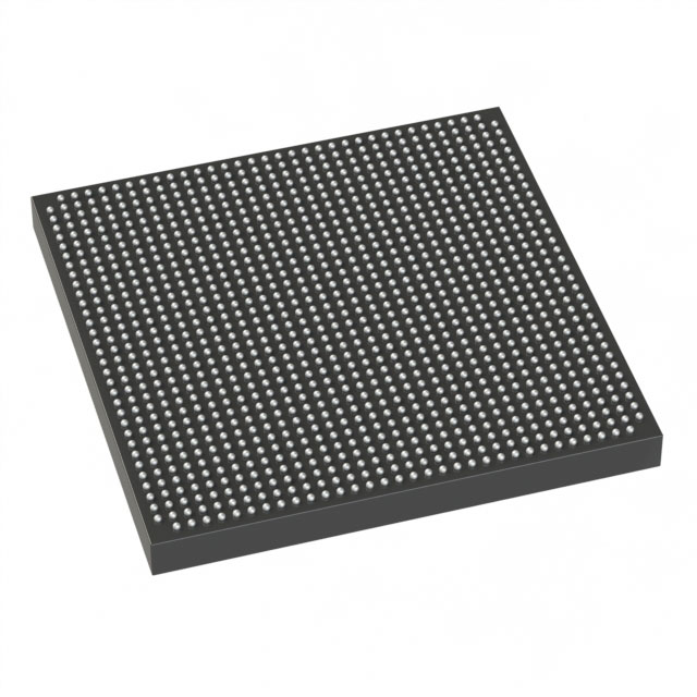
5SGXEA5K2F35I3G
| Part Description |
Stratix® V GX Field Programmable Gate Array (FPGA) IC 432 46080000 490000 1152-BBGA, FCBGA |
|---|---|
| Quantity | 615 Available (as of October 7, 2026) |
| Product Category | Field Programmable Gate Array (FPGA) |
|---|---|
| Manufacturer | Intel |
| Manufacturing Status | Active |
| Manufacturer Standard Lead Time | 26 Weeks |
| Datasheet |
Specifications & Environmental
| Device Package | 1152-FBGA (35x35) | Grade | Industrial | Operating Temperature | -40°C – 100°C | ||
|---|---|---|---|---|---|---|---|
| Package / Case | 1152-BBGA, FCBGA | Number of I/O | 432 | Voltage | 820 mV - 880 mV | ||
| Mounting Method | Surface Mount | RoHS Compliance | RoHS Compliant | REACH Compliance | REACH Unaffected | ||
| Moisture Sensitivity Level | 3 (168 Hours) | Number of LABs/CLBs | 185000 | Number of Logic Elements/Cells | 490000 | ||
| Number of Gates | N/A | ECCN | N/A | HTS Code | N/A | ||
| Qualification | N/A | Total RAM Bits | 46080000 |
Overview of 5SGXEA5K2F35I3G – Stratix® V GX FPGA, 490,000 Logic Elements, 1152‑BBGA
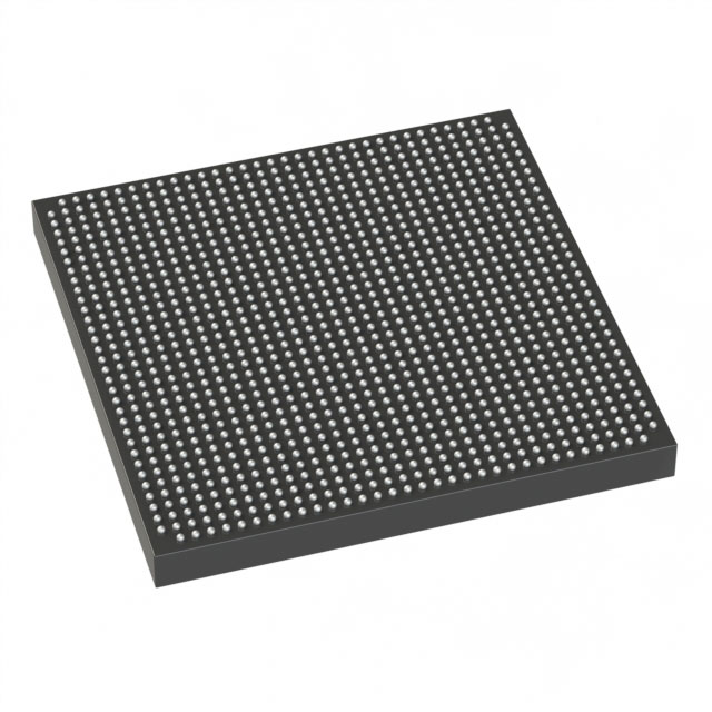
The 5SGXEA5K2F35I3G is an Intel Stratix® V GX field programmable gate array (FPGA) in a 1152‑BBGA (35×35) FCBGA package. It provides a high logic capacity and embedded memory footprint together with extensive I/O and industrial temperature rating for demanding systems.
Designed as part of the Stratix V family, the device supports the GX transceiver grades documented for Stratix V GX devices and targets designs that require large programmable logic, substantial on‑chip RAM, and broad I/O connectivity.
Key Features
- Core Logic Approximately 490,000 logic elements (cells) and 185,000 LABs/CLBs equivalent capacity for complex, high‑density logic implementation.
- Embedded Memory Approximately 46 Mbits of on‑chip RAM (46,080,000 total RAM bits) to support large FIFOs, buffers, and data‑intensive processing.
- I/O 432 user I/Os to support wide external interface routing and multi‑lane connectivity.
- Transceiver Capability (Series) Stratix V GX family device documentation specifies GX channel transceiver speed grades (examples include 14.1 Gbps and 12.5 Gbps), enabling high‑speed serial links where required by your design.
- Power Supply Core voltage supply range: 820 mV to 880 mV, enabling controlled power provisioning for core logic domains.
- Package 1152‑BBGA, FCBGA package (supplier device package listed as 1152‑FBGA 35×35) for high‑pin‑count, compact board integration.
- Temperature & Compliance Industrial temperature grade with operating range of –40 °C to 100 °C and RoHS compliance for regulatory adherence.
Typical Applications
- High‑bandwidth networking: Leverage the Stratix V GX family transceiver speed grades and 432 I/Os to implement multi‑lane interfaces and protocol offload in networking equipment.
- Signal processing and acceleration: Use the large logic capacity and ~46 Mbits of embedded RAM for FPGA‑based DSP, packet processing, and compute acceleration tasks.
- Prototyping and complex SoC integration: Deploy the device where extensive programmable logic, dense I/O routing, and industry temperature range are required for development platforms or embedded systems.
Unique Advantages
- High logic density: Nearly 490,000 logic elements enable integration of large digital designs without external logic expansion.
- Substantial on‑chip RAM: Approximately 46 Mbits of embedded memory reduces the need for external buffering and simplifies memory architecture.
- Extensive I/O count: 432 I/Os support wide parallel interfaces and flexible board partitioning for complex systems.
- Industrial temperature rating: –40 °C to 100 °C operation supports deployment in temperature‑challenging environments.
- High‑pin‑count FCBGA package: 1152‑BBGA (35×35) package provides dense connectivity in a compact footprint for space‑constrained boards.
- Standards compliance: RoHS compliance aligns the device with common environmental and regulatory requirements.
Why Choose 5SGXEA5K2F35I3G?
This Stratix V GX FPGA combines high logic capacity, significant embedded RAM, and broad I/O to address complex, high‑performance digital designs. Its industrial temperature rating and RoHS compliance make it suitable for applications that require robustness and regulatory alignment.
The device is appropriate for engineers and system designers who need a scalable programmable platform with transceiver‑capable family documentation, dense packaging, and a clear power‑supply specification for core domains.
If you would like pricing, availability, or a formal quote for 5SGXEA5K2F35I3G, request a quote or submit a procurement inquiry to receive further purchasing information and lead‑time details.





















Date Founded: 1968
Headquarters: Santa Clara, California, USA
Employees: 130,000+
Revenue: $54.23 Billion
Certifications and Memberships: ISO9001:2015, ISO14001:2015, ISO17025:2017, ISO27001:2022, ISO45001:2018, ISO50001:2018


