
5SGXEA7H3F35C2L
| Part Description |
Stratix® V GX Field Programmable Gate Array (FPGA) IC 552 51200000 622000 1152-BBGA, FCBGA |
|---|---|
| Quantity | 97 Available (as of June 18, 2026) |

| Product Category | Field Programmable Gate Array (FPGA) |
|---|---|
| Manufacturer | Intel |
| Manufacturing Status | Obsolete |
| Manufacturer Standard Lead Time | Contact Us |
| Datasheet |
Specifications & Environmental
| Device Package | 1152-FBGA (35x35) | Grade | Commercial | Operating Temperature | 0°C – 85°C | ||
|---|---|---|---|---|---|---|---|
| Package / Case | 1152-BBGA, FCBGA | Number of I/O | 552 | Voltage | 820 mV - 880 mV | ||
| Mounting Method | Surface Mount | RoHS Compliance | RoHS Compliant | REACH Compliance | REACH Unknown | ||
| Moisture Sensitivity Level | 3 (168 Hours) | Number of LABs/CLBs | 234720 | Number of Logic Elements/Cells | 622000 | ||
| Number of Gates | N/A | ECCN | 3A001A2C | HTS Code | 8542.39.0001 | ||
| Qualification | N/A | Total RAM Bits | 51200000 |
Overview of 5SGXEA7H3F35C2L – Stratix® V GX Field Programmable Gate Array (FPGA) IC
The 5SGXEA7H3F35C2L is a Stratix V GX family FPGA in an FCBGA package, designed for high-density, programmable logic integration. It pairs a large logic capacity with significant on-chip memory and extensive I/O to support complex digital designs and high-pin-count system integration.
As a commercial-grade Stratix V GX device, its specifications include core supply requirements, operating temperature range, and packaging optimized for surface-mount assembly. Detailed electrical and switching characteristics are documented in the Stratix V device datasheet.
Key Features
- High Logic Density Provides 622,000 logic elements for implementing large-scale digital designs and complex FPGA algorithms.
- Substantial Embedded Memory Includes 51,200,000 total RAM bits (approximately 51.2 Mbits) of on-chip memory for buffers, FIFOs, and embedded data storage.
- Extensive I/O Up to 552 device I/Os to support broad external interfacing and multi-channel connectivity.
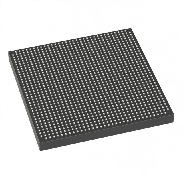
- Package and Mounting Surface-mount FCBGA package in a 1152-ball BBGA format; supplier device package listed as 1152-FBGA (35×35).
- Core Voltage Range Core voltage supply specified between 820 mV and 880 mV for device operation.
- Commercial Temperature Grade Rated for operation from 0 °C to 85 °C, suitable for commercial-environment applications.
- Environmental Compliance RoHS compliant.
Typical Applications
- High-density digital systems Leverage 622,000 logic elements and approximately 51.2 Mbits of embedded memory for complex logic, DSP functions, and algorithm acceleration.
- Multi-interface platforms Use the 552 I/Os to integrate with multiple peripherals, sensors, and high-pin-count connectors.
- Board-level integration FCBGA 1152-ball packaging and surface-mount mounting accommodate compact, high-performance PCB designs.
Unique Advantages
- Large programmable fabric: 622,000 logic elements enable scaling of logic-intensive designs without immediate need for additional devices.
- Significant on-chip memory: Approximately 51.2 Mbits of embedded RAM reduces dependence on external memory for buffering and data processing.
- High I/O count: 552 I/Os simplify board routing for multi-channel systems and complex I/O configurations.
- Surface-mount FCBGA packaging: Compact 1152-ball FCBGA supports dense board layouts and reliable soldered connections for production assemblies.
- Clear commercial operating envelope: Specified 0 °C to 85 °C operating range and 820–880 mV core supply provide predictable integration parameters for commercial designs.
- RoHS compliant: Meets environmental requirements for lead-free and restricted-substance assembly processes.
Why Choose 5SGXEA7H3F35C2L?
The 5SGXEA7H3F35C2L delivers a combination of high logic capacity, ample embedded memory, and a large number of I/Os in a production-ready FCBGA package. Its specifications support complex, high-density FPGA designs where on-chip resources and I/O density are primary considerations. Engineers targeting commercial-grade systems that require scalable logic, substantial on-chip RAM, and robust packaging will find this Stratix V GX device aligns with those requirements.
Backed by the Stratix V device documentation, this FPGA is suitable for designs that demand clearly defined electrical characteristics and proven architecture-level information from the device family datasheet.
If you would like pricing, availability, or to submit a request for a quote for 5SGXEA7H3F35C2L, please request a quote or contact sales through your usual procurement channel.


Date Founded: 1968
Headquarters: Santa Clara, California, USA
Employees: 130,000+
Revenue: $54.23 Billion
Certifications and Memberships: ISO9001:2015, ISO14001:2015, ISO17025:2017, ISO27001:2022, ISO45001:2018, ISO50001:2018


