
5SGXEA7K3F40C4N
| Part Description |
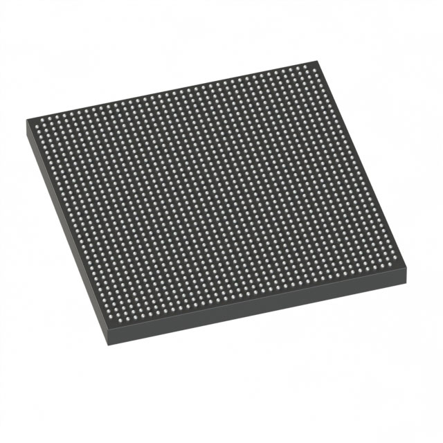
Stratix® V GX Field Programmable Gate Array (FPGA) IC 696 51200000 622000 1517-BBGA, FCBGA |
|---|---|
| Quantity | 57 Available (as of June 12, 2026) |

| Product Category | Field Programmable Gate Array (FPGA) |
|---|---|
| Manufacturer | Intel |
| Manufacturing Status | Obsolete |
| Manufacturer Standard Lead Time | Contact Us |
| Datasheet |
Specifications & Environmental
| Device Package | 1517-FBGA (40x40) | Grade | Commercial | Operating Temperature | 0°C – 85°C | ||
|---|---|---|---|---|---|---|---|
| Package / Case | 1517-BBGA, FCBGA | Number of I/O | 696 | Voltage | 820 mV - 880 mV | ||
| Mounting Method | Surface Mount | RoHS Compliance | RoHS Compliant | REACH Compliance | REACH Unknown | ||
| Moisture Sensitivity Level | 3 (168 Hours) | Number of LABs/CLBs | 234720 | Number of Logic Elements/Cells | 622000 | ||
| Number of Gates | N/A | ECCN | 3A001A2C | HTS Code | 8542.39.0001 | ||
| Qualification | N/A | Total RAM Bits | 51200000 |
Overview of 5SGXEA7K3F40C4N – Stratix® V GX Field Programmable Gate Array (FPGA) IC
The 5SGXEA7K3F40C4N is an Intel Stratix V GX family FPGA supplied in a 1517-BBGA (FCBGA) package for surface-mount applications. It provides 622,000 logic elements and approximately 51.2 Mbits of embedded memory, making it suitable for high-density programmable-logic designs that require significant on-chip logic and memory resources.
Designed as a commercial-grade device (0 °C to 85 °C), this Stratix V GX device is part of a series that includes high-speed transceiver options and a range of core/transceiver speed grades for performance-scalable designs.
Key Features
- Core Logic Capacity 622,000 logic elements to support complex, high-density digital designs and custom hardware accelerators.
- Embedded Memory Approximately 51.2 Mbits of on-chip RAM for buffering, on-chip data storage, and memory-intensive algorithms.
- I/O Density 696 I/O pins to accommodate high-pin-count interfaces and dense external connectivity.
- Package & Mounting 1517-BBGA (FCBGA) supplier device package (1517-FBGA, 40×40) with surface-mount mounting for compact board integration.
- Power and Voltage Specified core supply range of 0.820 V to 0.880 V to match platform power rails and support low-voltage core implementations.
- Operating Range & Grade Commercial temperature grade with an operating range of 0 °C to 85 °C for standard embedded and enterprise applications.
- Standards Compliance RoHS compliant to meet lead-free manufacturing requirements.
- Stratix V GX Series Capabilities Part of the Stratix V GX family, which includes devices with selectable transceiver speed grades for multi-gigabit channel support (series-level specification).
Typical Applications
- High-density logic implementations Custom compute blocks and hardware accelerators that require large logic and routing resources.
- Memory-intensive processing On-chip buffering, packet handling, and algorithmic data paths leveraging ~51.2 Mbits of embedded RAM.
- High-pin-count interface systems Complex I/O subsystems and board-level integrations that require hundreds of I/O signals.
Unique Advantages
- Substantial logic capacity: 622,000 logic elements enable implementation of large-scale logic designs without immediate need for multi-FPGA partitioning.
- Significant on-chip memory: Approximately 51.2 Mbits of embedded RAM reduces dependence on external memory for many buffering and DSP tasks.
- High I/O count: 696 I/O pins provide flexibility for dense peripheral and high-channel-count interfacing.
- Compact BGA footprint: 1517-BBGA FCBGA package supports high-density PCB layouts while preserving thermal and mechanical robustness for surface-mount assembly.
- Controlled core voltage range: 0.820 V–0.880 V specification allows predictable power-supply planning for core domains.
- Commercial temperature grade: 0 °C–85 °C operation fits a wide range of commercial and enterprise use cases.
Why Choose 5SGXEA7K3F40C4N?
The 5SGXEA7K3F40C4N delivers a combination of large logic capacity, substantial embedded memory, and a high I/O count in a compact FCBGA package—positioning it for demanding, high-density FPGA implementations. As part of the Stratix V GX family, it aligns with series-level transceiver capabilities and speed-grade options for designs that may require multi-gigabit channel support.
This device is appropriate for engineering teams targeting scalable, high-performance programmable logic solutions in commercial environments where on-chip memory and I/O density are critical to simplifying board-level design and reducing external component count.
Request a quote or submit a request for pricing and availability to evaluate the 5SGXEA7K3F40C4N for your next design project.


Date Founded: 1968
Headquarters: Santa Clara, California, USA
Employees: 130,000+
Revenue: $54.23 Billion
Certifications and Memberships: ISO9001:2015, ISO14001:2015, ISO17025:2017, ISO27001:2022, ISO45001:2018, ISO50001:2018


