
5SGXEA9N3F45C2G
| Part Description |
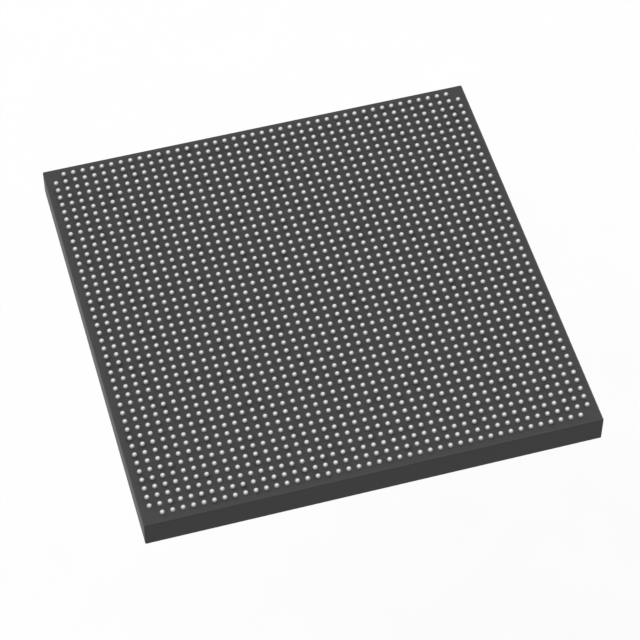
Stratix® V GX Field Programmable Gate Array (FPGA) IC 840 53248000 840000 1932-BBGA, FCBGA |
|---|---|
| Quantity | 164 Available (as of June 14, 2026) |

| Product Category | Field Programmable Gate Array (FPGA) |
|---|---|
| Manufacturer | Intel |
| Manufacturing Status | Active |
| Manufacturer Standard Lead Time | 26 Weeks |
| Datasheet |
Specifications & Environmental
| Device Package | 1932-FBGA, FC (45x45) | Grade | Commercial | Operating Temperature | 0°C – 85°C | ||
|---|---|---|---|---|---|---|---|
| Package / Case | 1932-BBGA, FCBGA | Number of I/O | 840 | Voltage | 870 mV - 930 mV | ||
| Mounting Method | Surface Mount | RoHS Compliance | RoHS Compliant | REACH Compliance | REACH Unaffected | ||
| Moisture Sensitivity Level | 3 (168 Hours) | Number of LABs/CLBs | 317000 | Number of Logic Elements/Cells | 840000 | ||
| Number of Gates | N/A | ECCN | N/A | HTS Code | N/A | ||
| Qualification | N/A | Total RAM Bits | 53248000 |
Overview of 5SGXEA9N3F45C2G – Stratix® V GX Field Programmable Gate Array (FPGA), 840,000 logic elements
The 5SGXEA9N3F45C2G is a high-density Stratix V GX FPGA in a 1932-ball FCBGA package, optimized for demanding programmable-logic applications. As a member of the Stratix V GX family, the device provides large logic capacity, substantial on-chip memory, and abundant I/O for complex digital designs.
Designed for commercial-grade systems, this FPGA targets applications that require high logic density, extensive embedded memory, and high pin count in a surface-mount FCBGA package.
Key Features
- Logic Capacity Provides 840,000 logic elements to implement large-scale digital designs and complex system logic.
- Embedded Memory Approximately 53.25 Mbits of on-chip RAM for buffering, frame storage, and data-path designs.
- I/O Density 840 user I/O pins to support wide parallel interfaces and multi-channel connectivity.
- Package Surface-mount 1932-BBGA (FCBGA) with a 45×45 mm supplier device package footprint for high-pin-count, compact board layouts.
- Power Core supply voltage range of 870 mV to 930 mV suitable for Stratix V GX core operation modes.
- Temperature Grade Commercial operating range from 0 °C to 85 °C for standard commercial applications.
- Environmental Compliance RoHS compliant to meet common environmental and manufacturing requirements.
- Series-level High-speed Transceiver Support Stratix V GX devices feature high-speed transceivers as documented for the series (see datasheet for supported transceiver speed grades and configurations).
Typical Applications
- High-speed communications Large logic capacity and series-level high-speed transceivers make the device suitable for multi-channel backplane and networking functions.
- Data processing and acceleration Substantial on-chip RAM and high logic density support custom accelerators, packet processing, and throughput-intensive pipelines.
- Advanced digital systems High I/O count and dense logic enable implementation of complex controllers, interface bridging, and system-level integration.
- Prototyping and platform development The combination of logic, memory, and I/O resources supports system prototyping and evaluation of large designs on a single device.
Unique Advantages
- High logic integration: 840,000 logic elements reduce the need for multi-device partitioning and simplify system architecture.
- Large embedded memory: Approximately 53.25 Mbits of on-chip RAM provides ample capacity for buffers, FIFOs, and data-path storage.
- Extensive I/O capability: 840 I/O pins allow dense parallel interfacing and flexible I/O allocation for complex systems.
- Compact, high-pin-count package: 1932-ball FCBGA in a 45×45 mm footprint supports high-density board designs while keeping component count low.
- Commercial temperature and RoHS compliance: Rated for 0 °C to 85 °C operation and RoHS compliant for standard commercial production environments.
- Series-level transceiver options: Stratix V GX family documentation describes high-speed transceiver capabilities for designs that require serial connectivity (refer to the datasheet for details).
Why Choose 5SGXEA9N3F45C2G?
The 5SGXEA9N3F45C2G combines very high logic density, significant embedded memory, and a large number of I/Os in a single commercial-grade FCBGA package—making it a practical choice for designers implementing complex, high-performance digital systems. Its package and power characteristics support compact, high-pin-count board layouts while maintaining the power envelope expected of Stratix V GX core operation.
This device is well suited for teams developing high-throughput communications equipment, data-path accelerators, or system prototypes that require scalable logic resources and series-level high-speed transceiver capability as described in the Stratix V GX documentation.
Request a quote or submit an inquiry to receive pricing and availability information for the 5SGXEA9N3F45C2G.


Date Founded: 1968
Headquarters: Santa Clara, California, USA
Employees: 130,000+
Revenue: $54.23 Billion
Certifications and Memberships: ISO9001:2015, ISO14001:2015, ISO17025:2017, ISO27001:2022, ISO45001:2018, ISO50001:2018


