
5SGXEA9N3F45C2L
| Part Description |
Stratix® V GX Field Programmable Gate Array (FPGA) IC 840 53248000 840000 1932-BBGA, FCBGA |
|---|---|
| Quantity | 128 Available (as of June 14, 2026) |

| Product Category | Field Programmable Gate Array (FPGA) |
|---|---|
| Manufacturer | Intel |
| Manufacturing Status | Obsolete |
| Manufacturer Standard Lead Time | Contact Us |
| Datasheet |
Specifications & Environmental
| Device Package | 1932-FBGA, FC (45x45) | Grade | Commercial | Operating Temperature | 0°C – 85°C | ||
|---|---|---|---|---|---|---|---|
| Package / Case | 1932-BBGA, FCBGA | Number of I/O | 840 | Voltage | 820 mV - 880 mV | ||
| Mounting Method | Surface Mount | RoHS Compliance | RoHS Compliant | REACH Compliance | REACH Unknown | ||
| Moisture Sensitivity Level | 3 (168 Hours) | Number of LABs/CLBs | 317000 | Number of Logic Elements/Cells | 840000 | ||
| Number of Gates | N/A | ECCN | 3A001A2C | HTS Code | 8542.39.0001 | ||
| Qualification | N/A | Total RAM Bits | 53248000 |
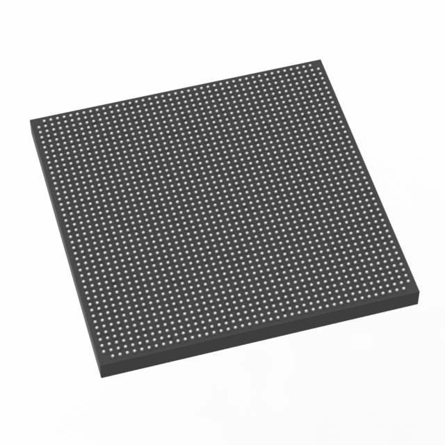
Overview of 5SGXEA9N3F45C2L – Stratix® V GX FPGA, 840K logic elements, 1932-BBGA
The 5SGXEA9N3F45C2L is a Stratix® V GX Field Programmable Gate Array (FPGA) in a 1932-BBGA FCBGA package designed for high-density, commercial-grade logic integration. With 840,000 logic elements and approximately 53 Mbits of embedded memory, this device targets complex digital designs that require large on-chip resources and a high I/O count.
Engineered for surface-mount PCB implementations, the device offers a low-voltage core operating range and commercial temperature rating, making it suitable for demanding system and board-level applications where integration density and efficient power delivery are key considerations.
Key Features
- Logic Capacity 840,000 logic elements to support large-scale digital designs and extensive custom logic implementation.
- Embedded Memory Approximately 53 Mbits of on-chip RAM for buffering, state storage, and memory-intensive logic functions.
- I/O Count 840 user I/O pins to accommodate wide parallel interfaces and diverse peripheral connections.
- Power and Core Voltage Core supply voltage range 820 mV to 880 mV, enabling operation within a defined low-voltage domain.
- Package and Mounting 1932-BBGA (FCBGA) package; supplier device package listed as 1932-FBGA, FC (45×45). Surface-mount for compact board-level integration.
- Operating Grade and Temperature Commercial grade with an operating temperature range of 0 °C to 85 °C.
- Standards Compliance RoHS compliant.
Typical Applications
- High-density digital systems Implement complex processing pipelines and custom accelerators using the device's large logic and memory resources.
- High-channel I/O designs Use the 840 available I/O pins for wide data buses, multi-channel interfaces, or extensive peripheral connectivity.
- Embedded memory-centric functions Leverage approximately 53 Mbits of on-chip RAM for buffering, packet processing, or stateful logic without external memory dependence.
Unique Advantages
- High integration density: 840,000 logic elements reduce the need for multiple devices and simplify system architecture.
- Substantial on-chip memory: Approximately 53 Mbits of embedded RAM supports large data structures and reduces external memory traffic.
- Extensive I/O capability: 840 I/O pins provide flexibility for complex interface requirements and multi-channel I/O designs.
- Compact surface-mount package: 1932-BBGA FCBGA enables dense board layouts while providing a high pin count footprint.
- Defined low-voltage core: 820–880 mV supply range supports predictable power-domain design and regulator selection.
- Commercial-grade reliability: Rated for 0 °C to 85 °C operation and RoHS compliant for mainstream electronic products.
Why Choose 5SGXEA9N3F45C2L?
The 5SGXEA9N3F45C2L combines very large logic capacity, substantial embedded memory, and a high I/O count in a single commercial-grade Stratix V GX FPGA package. It is positioned for designers who need to consolidate complex digital functions, implement memory-heavy logic, and support extensive peripheral connectivity on compact PCBs.
For development teams and procurement focused on scalable, high-density FPGA solutions, this device offers a clear hardware platform with defined electrical and environmental parameters to support board-level integration and system design continuity.
Request a quote or submit a procurement inquiry to evaluate the 5SGXEA9N3F45C2L for your next design.


Date Founded: 1968
Headquarters: Santa Clara, California, USA
Employees: 130,000+
Revenue: $54.23 Billion
Certifications and Memberships: ISO9001:2015, ISO14001:2015, ISO17025:2017, ISO27001:2022, ISO45001:2018, ISO50001:2018


