
5SGXEABK3H40I4N
| Part Description |
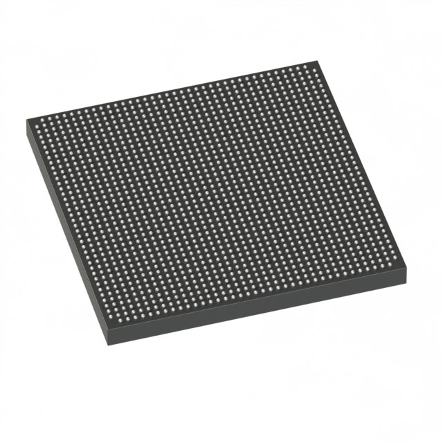
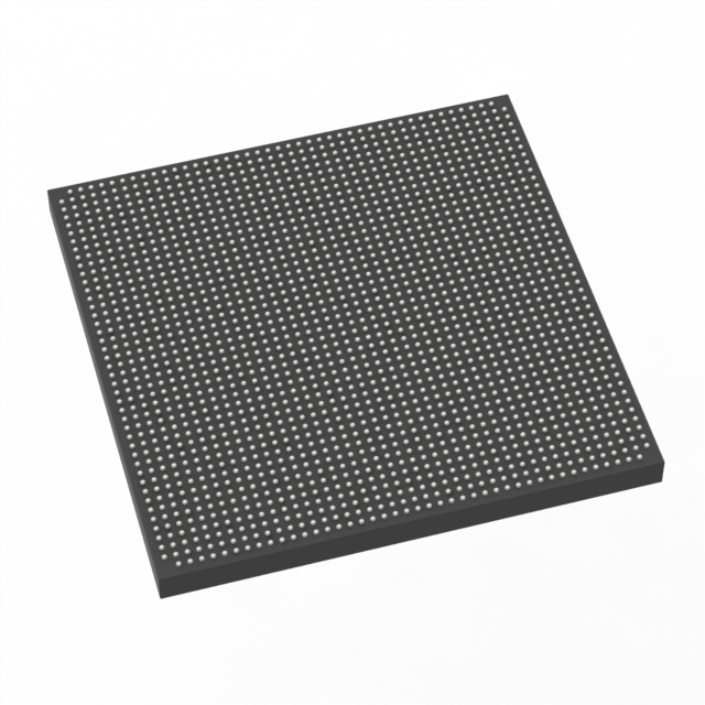
Stratix® V GX Field Programmable Gate Array (FPGA) IC 696 53248000 952000 1517-BBGA, FCBGA |
|---|---|
| Quantity | 817 Available (as of June 9, 2026) |

| Product Category | Field Programmable Gate Array (FPGA) |
|---|---|
| Manufacturer | Intel |
| Manufacturing Status | Obsolete |
| Manufacturer Standard Lead Time | Contact Us |
| Datasheet |
Specifications & Environmental
| Device Package | 1517-HBGA (45x45) | Grade | Industrial | Operating Temperature | -40°C – 100°C | ||
|---|---|---|---|---|---|---|---|
| Package / Case | 1517-BBGA, FCBGA | Number of I/O | 696 | Voltage | 820 mV - 880 mV | ||
| Mounting Method | Surface Mount | RoHS Compliance | RoHS Compliant | REACH Compliance | REACH Unknown | ||
| Moisture Sensitivity Level | 3 (168 Hours) | Number of LABs/CLBs | 359200 | Number of Logic Elements/Cells | 952000 | ||
| Number of Gates | N/A | ECCN | 3A001A2C | HTS Code | 8542.39.0001 | ||
| Qualification | N/A | Total RAM Bits | 53248000 |
Overview of 5SGXEABK3H40I4N – Stratix® V GX Field Programmable Gate Array (FPGA) IC
The 5SGXEABK3H40I4N is a Stratix® V GX FPGA device provided in a 1517-BBGA FCBGA package. It delivers very large programmable logic capacity and embedded memory, packaged for surface-mount board assembly and rated for industrial temperature operation.
With 952,000 logic elements and approximately 53 Mbits of embedded memory, this device targets high-density, high-channel-count designs that require extensive on-chip resources and a wide range of I/O connectivity.
Key Features
- Logic Capacity 952,000 logic elements for large-scale programmable logic and complex design implementation.
- Embedded Memory Approximately 53 Mbits of total on-chip RAM bits to support large buffering, state storage, and memory-intensive functions.
- I/O Density 696 user I/O pins to support dense board-level interfaces and multi-channel connectivity.
- Transceiver Family Capability Member of the Stratix V GX family; the series documentation includes transceiver speed-grade information for high-speed channels at the family level.
- Power and Core Voltage Core voltage supply in the range of 820 mV to 880 mV, enabling design planning for the device’s power domain.
- Package and Mounting 1517-BBGA (FCBGA) package; supplier device package listed as 1517-HBGA (45×45) and intended for surface-mount assembly.
- Industrial Temperature Grade Rated operating temperature range −40°C to 100°C for deployment in industrial environments.
- Compliance RoHS compliant.
Typical Applications
- High-density programmable logic Use the device’s 952,000 logic elements and large embedded RAM to implement complex, large-scale custom logic architectures.
- High I/O and interface consolidation Leverage 696 I/Os to integrate multiple board-level interfaces and consolidate system connectivity on a single FPGA.
- Industrial-grade systems The −40°C to 100°C operating range makes this device suitable for industrial applications that require extended temperature tolerance.
- Designs requiring on-chip memory Approximately 53 Mbits of embedded RAM provides significant on-chip storage for buffering, FIFOs, and state machines.
Unique Advantages
- Very large programmable capacity: 952,000 logic elements enable consolidation of multiple functions into a single FPGA, reducing component count.
- Substantial embedded memory: Approximately 53 Mbits of on-chip RAM supports memory-heavy algorithms and minimizes external memory dependencies.
- Extensive I/O complement: 696 I/Os provide flexibility for high-channel-count designs and dense interface routing.
- Industrial temperature rating: Rated from −40°C to 100°C to accommodate applications deployed in demanding thermal environments.
- Surface-mount, high-density package: 1517-BBGA (1517-HBGA supplier designation, 45×45) enables compact PCB integration for space-constrained systems.
- Regulatory compliance: RoHS compliance supports environmentally conscious product builds.
Why Choose 5SGXEABK3H40I4N?
The 5SGXEABK3H40I4N combines very large logic capacity, significant embedded memory, and a high I/O count in a single industrial-grade, surface-mount package. These characteristics make it well suited to engineers building consolidated, resource-intensive FPGA designs that require substantial on-chip resources and robust thermal tolerance.
As part of the Stratix V GX family, this device aligns with the family-level electrical and transceiver specifications documented for Stratix V devices, allowing designers to reference the series documentation for device-level electrical and switching characteristics during development.
Request a quote or submit an inquiry for pricing and availability to begin integrating the 5SGXEABK3H40I4N into your design workflow.


Date Founded: 1968
Headquarters: Santa Clara, California, USA
Employees: 130,000+
Revenue: $54.23 Billion
Certifications and Memberships: ISO9001:2015, ISO14001:2015, ISO17025:2017, ISO27001:2022, ISO45001:2018, ISO50001:2018


