
5SGXEABN1F45C2G
| Part Description |
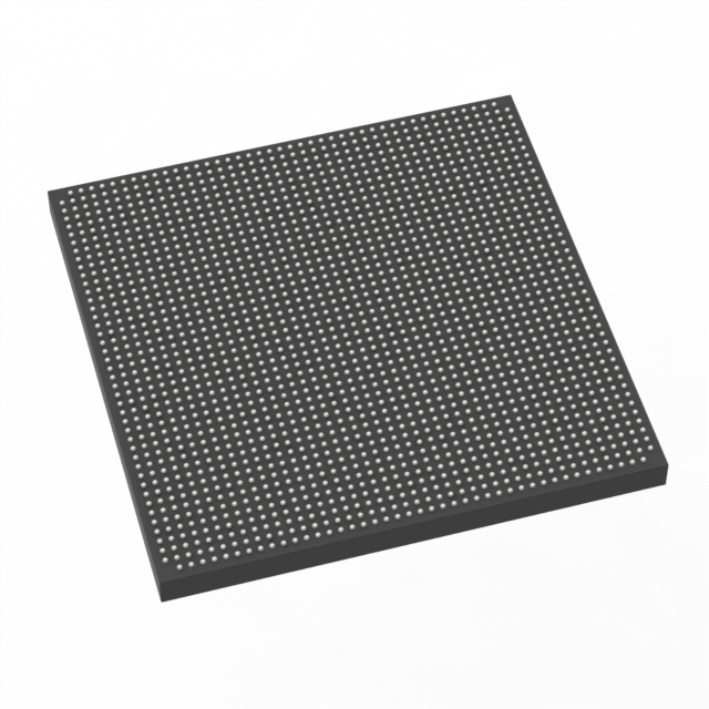
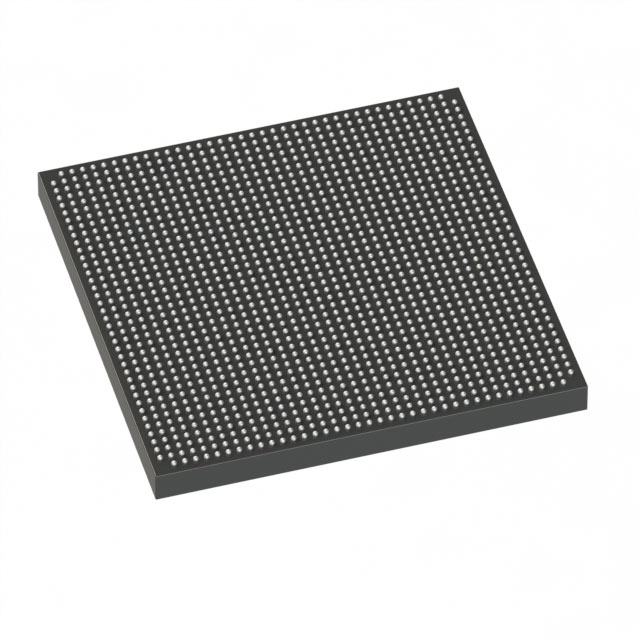
Stratix® V GX Field Programmable Gate Array (FPGA) IC 840 53248000 952000 1932-BBGA, FCBGA |
|---|---|
| Quantity | 961 Available (as of June 15, 2026) |
| Product Category | Field Programmable Gate Array (FPGA) |
|---|---|
| Manufacturer | Intel |
| Manufacturing Status | Active |
| Manufacturer Standard Lead Time | 26 Weeks |
| Datasheet |
Specifications & Environmental
| Device Package | 1932-FBGA, FC (45x45) | Grade | Commercial | Operating Temperature | 0°C – 85°C | ||
|---|---|---|---|---|---|---|---|
| Package / Case | 1932-BBGA, FCBGA | Number of I/O | 840 | Voltage | 870 mV - 930 mV | ||
| Mounting Method | Surface Mount | RoHS Compliance | RoHS Compliant | REACH Compliance | REACH Unaffected | ||
| Moisture Sensitivity Level | 3 (168 Hours) | Number of LABs/CLBs | 359200 | Number of Logic Elements/Cells | 952000 | ||
| Number of Gates | N/A | ECCN | N/A | HTS Code | N/A | ||
| Qualification | N/A | Total RAM Bits | 53248000 |
Overview of 5SGXEABN1F45C2G – Stratix® V GX Field Programmable Gate Array (FPGA) IC, 1932-BBGA FCBGA
The 5SGXEABN1F45C2G is a Stratix V GX field programmable gate array (FPGA) from Intel. It delivers substantial on-chip logic and memory resources in a high-density FCBGA package tailored for complex, programmable logic designs.
Key on-chip resources include 952,000 logic elements and approximately 53 Mbits of embedded memory, combined with 840 user I/Os and Stratix V GX transceiver speed grades (up to 14.1 Gbps per GX channel as documented for the family). The device is supplied in a 1932-BBGA surface-mount package and is offered as a commercial-grade part (0 °C to 85 °C).
Key Features
- Core logic capacity — 952,000 logic elements provide large programmable logic resources for high-density designs.
- Embedded memory — Approximately 53 Mbits of on-chip RAM for buffering, lookup tables, and data storage.
- I/O density — 840 user I/Os to support broad system interfacing and parallel connectivity.
- High-speed transceivers (family) — Stratix V GX transceiver speed grades for the device family include channel rates up to 14.1 Gbps as documented in the device datasheet.
- Power — core supply — Core voltage supply range of 870 mV to 930 mV to match targeted power domains.
- Package & mounting — 1932-BBGA (FCBGA) supplier device package: 1932-FBGA, FC (45×45); surface-mount mounting type.
- Commercial operating range — Rated for 0 °C to 85 °C operating temperature and specified as commercial grade.
- Compliance — RoHS compliant.
Typical Applications
- High-speed communications — Use the device where Stratix V GX transceiver grades and dense logic are needed for serial links and protocol handling.
- Data processing and acceleration — Large logic and embedded memory capacity support custom data-paths, buffering, and hardware acceleration functions.
- Prototyping and complex system integration — High I/O count and substantial logic resources enable development and integration of complex SoC prototypes and platform designs.
- Test and measurement systems — Combine high logic density and flexible I/O to implement custom measurement, signal processing, and control logic.
Unique Advantages
- High logic density: 952,000 logic elements reduce the need for multi-device partitioning in large designs.
- Significant on-chip memory: Approximately 53 Mbits of embedded RAM supports sizable buffering and local data storage.
- Broad I/O capability: 840 I/Os provide flexibility for parallel interfaces, wide buses, and complex board-level connections.
- Surface-mount FCBGA package: 1932-BBGA (45×45) packaging enables high-density board integration in surface-mount assemblies.
- Commercial temperature rating: 0 °C to 85 °C operation aligns with a wide range of commercial electronics applications.
- Documented family performance: Backed by Stratix V device datasheet documentation covering electrical and switching characteristics relevant to design and validation.
Why Choose 5SGXEABN1F45C2G?
The 5SGXEABN1F45C2G positions itself as a high-capacity Stratix V GX FPGA option for designers requiring extensive logic resources, ample on-chip memory, and dense I/O in a single surface-mount package. Its combination of 952,000 logic elements, approximately 53 Mbits of embedded RAM, and 840 I/Os makes it suitable for complex programmable systems where consolidation and flexibility matter.
As a commercial-grade Stratix V GX device with documented electrical and transceiver characteristics, it is appropriate for development, prototyping, and deployment in systems that operate within the specified voltage and temperature ranges. The device is RoHS compliant and supplied in a 1932-BBGA FCBGA package for high-density board-level integration.
Request a quote or submit an inquiry for pricing and availability for the 5SGXEABN1F45C2G FPGA. Our team can provide lead-time information and assist with technical documentation references for design integration.


Date Founded: 1968
Headquarters: Santa Clara, California, USA
Employees: 130,000+
Revenue: $54.23 Billion
Certifications and Memberships: ISO9001:2015, ISO14001:2015, ISO17025:2017, ISO27001:2022, ISO45001:2018, ISO50001:2018


