
5SGXEB6R2F43C2
| Part Description |
Stratix® V GX Field Programmable Gate Array (FPGA) IC 600 53248000 597000 1760-BBGA, FCBGA |
|---|---|
| Quantity | 1,729 Available (as of June 15, 2026) |

| Product Category | Field Programmable Gate Array (FPGA) |
|---|---|
| Manufacturer | Intel |
| Manufacturing Status | Obsolete |
| Manufacturer Standard Lead Time | Contact Us |
| Datasheet |
Specifications & Environmental
| Device Package | 1760-FCBGA (42.5x42.5) | Grade | Commercial | Operating Temperature | 0°C – 85°C | ||
|---|---|---|---|---|---|---|---|
| Package / Case | 1760-BBGA, FCBGA | Number of I/O | 600 | Voltage | 870 mV - 930 mV | ||
| Mounting Method | Surface Mount | RoHS Compliance | RoHS Compliant | REACH Compliance | REACH Unknown | ||
| Moisture Sensitivity Level | 3 (168 Hours) | Number of LABs/CLBs | 225400 | Number of Logic Elements/Cells | 597000 | ||
| Number of Gates | N/A | ECCN | 3A001A2C | HTS Code | 8542.39.0001 | ||
| Qualification | N/A | Total RAM Bits | 53248000 |
Overview of 5SGXEB6R2F43C2 – Stratix® V GX FPGA, 597,000 logic elements, ~53.248 Mbits RAM, 600 I/Os
The 5SGXEB6R2F43C2 is a Stratix® V GX field-programmable gate array (FPGA) IC offering very large logic capacity and on-chip memory for high-density designs. It combines 597,000 logic elements with approximately 53.248 Mbits of embedded RAM and 600 user I/Os to support complex digital systems and high I/O integration.
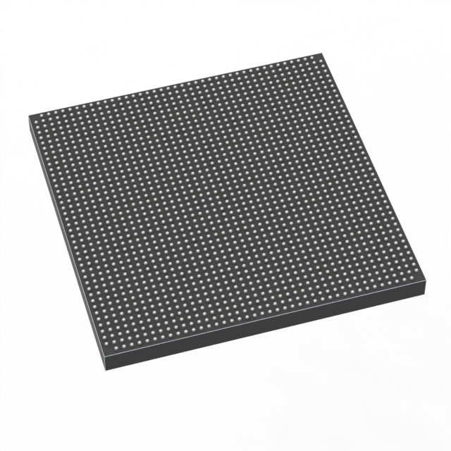
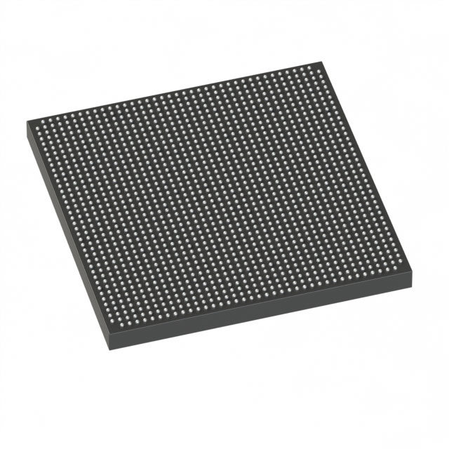
Housed in a 1760-ball FCBGA (42.5 × 42.5 mm) surface-mount package and rated for commercial operation (0 °C to 85 °C), this device targets applications that require substantial logic, abundant I/O, and series-level Stratix V GX transceiver capabilities as documented in the family datasheet.
Key Features
- Logic Capacity 597,000 logic elements provide extensive fabric for implementing large state machines, datapaths, and custom accelerators.
- Logic Array Blocks 225,400 logic array blocks as specified for detailed mapping and resource planning.
- Embedded Memory Approximately 53.248 Mbits of on-chip RAM to support large buffers, FIFOs, and on-chip data storage.
- I/O Density 600 user I/O pins enable high-connectivity designs requiring many external interfaces, parallel buses, or multiple high-pin-count peripherals.
- Package and Mounting 1760-FCBGA (42.5 × 42.5 mm) surface-mount package for high-density board integration.
- Power Supply Core voltage supply range 870 mV to 930 mV for system power planning and regulator selection.
- Operating Conditions Commercial grade with an operating temperature range of 0 °C to 85 °C and RoHS compliance.
- Series Transceiver Information Stratix V GX family transceiver speed grades are documented in the series datasheet (family-level information includes GX channel grades up to 14.1 Gbps), useful when planning high-speed serial links.
Typical Applications
- High-density digital processing Large logic and memory resources enable implementation of complex data-paths, custom accelerators, and timing-critical processing chains.
- Network and communications equipment High I/O count and family-level transceiver capability support multiport and high-bandwidth interface designs.
- Prototyping and system integration Extensive logic and on-chip memory make the device suitable for emulation, FPGA prototyping, and integration of large HDL designs.
- Signal processing and packet buffering Substantial embedded RAM capacity supports buffers, FIFOs, and intermediate data storage for DSP workloads.
Unique Advantages
- High integration density: With 597,000 logic elements and large embedded RAM, the device consolidates complex functions into a single FPGA, reducing external component count.
- Abundant I/O resources: 600 user I/Os allow direct interfacing to many peripherals and parallel interfaces without extensive multiplexing.
- Clear power envelope: Defined core voltage range (870 mV–930 mV) simplifies power supply design and regulator selection.
- Commercial temperature suitability: Rated for 0 °C to 85 °C, appropriate for a wide range of commercial and enterprise applications.
- Standard surface-mount packaging: 1760-FCBGA (42.5 × 42.5 mm) enables dense PCB layouts and compatibility with common high-pin-count assembly processes.
- RoHS compliant: Conforms to RoHS requirements for lead-free assembly and regulatory alignment.
Why Choose 5SGXEB6R2F43C2?
The 5SGXEB6R2F43C2 positions itself for designs that demand very large logic capacity, significant embedded memory, and high I/O density in a single commercial-grade FPGA package. Its package and power specifications help streamline board-level integration while the series-level Stratix V GX transceiver information supports planning for high-speed serial interfaces.
Choose this device for complex system integration, high-throughput data paths, and FPGA-based prototyping where consolidated logic, memory, and I/O reduce BOM complexity and simplify system architecture.
If you would like pricing, availability, or a formal quote for 5SGXEB6R2F43C2, request a quote or submit an inquiry and our team will respond with next steps.


Date Founded: 1968
Headquarters: Santa Clara, California, USA
Employees: 130,000+
Revenue: $54.23 Billion
Certifications and Memberships: ISO9001:2015, ISO14001:2015, ISO17025:2017, ISO27001:2022, ISO45001:2018, ISO50001:2018


