
5SGXEB6R2F43C2G
| Part Description |
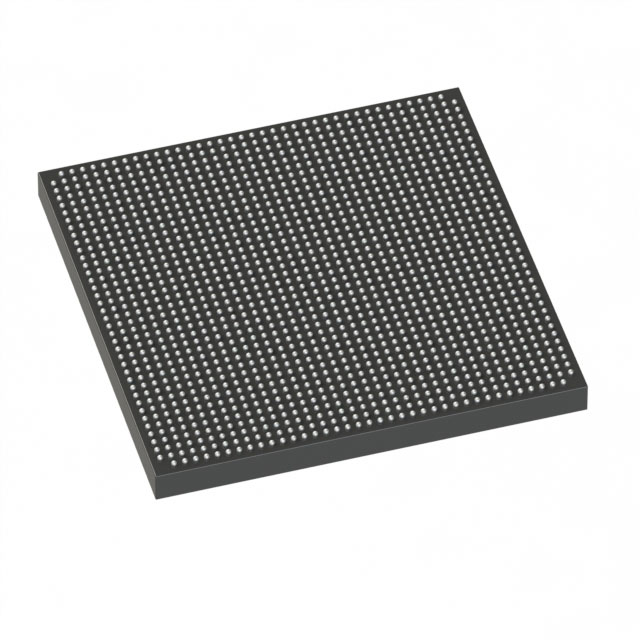
Stratix® V GX Field Programmable Gate Array (FPGA) IC 600 53248000 597000 1760-BBGA, FCBGA |
|---|---|
| Quantity | 1,253 Available (as of June 14, 2026) |

| Product Category | Field Programmable Gate Array (FPGA) |
|---|---|
| Manufacturer | Intel |
| Manufacturing Status | Active |
| Manufacturer Standard Lead Time | 26 Weeks |
| Datasheet |
Specifications & Environmental
| Device Package | 1760-FCBGA (42.5x42.5) | Grade | Commercial | Operating Temperature | 0°C – 85°C | ||
|---|---|---|---|---|---|---|---|
| Package / Case | 1760-BBGA, FCBGA | Number of I/O | 600 | Voltage | 870 mV - 930 mV | ||
| Mounting Method | Surface Mount | RoHS Compliance | RoHS Compliant | REACH Compliance | REACH Unaffected | ||
| Moisture Sensitivity Level | 3 (168 Hours) | Number of LABs/CLBs | 225400 | Number of Logic Elements/Cells | 597000 | ||
| Number of Gates | N/A | ECCN | N/A | HTS Code | N/A | ||
| Qualification | N/A | Total RAM Bits | 53248000 |
Overview of 5SGXEB6R2F43C2G – Stratix® V GX FPGA, 1760-FCBGA
The 5SGXEB6R2F43C2G is an Intel Stratix® V GX field programmable gate array (FPGA) in a 1760-ball FCBGA package. It delivers very large programmable logic capacity and on-chip memory for complex digital designs while providing extensive I/O for advanced system integration.
This commercial-grade device is suited for applications that require substantial logic resources, significant embedded RAM, and high I/O counts, while operating within standard commercial temperature and core-voltage ranges.
Key Features
- Core Capacity Approximately 597,000 logic elements, enabling large, high-density designs and complex logic implementation.
- Embedded Memory Approximately 53.25 Mbits of embedded memory (on-chip RAM) to support buffers, FIFOs, and data storage for stateful logic and processing.
- I/O Up to 600 user I/O pins for broad peripheral and system interfacing.
- Transceiver / Family Capabilities As a Stratix V GX device family member, the series documentation includes GX transceiver speed grade information (family-level details available in the device datasheet).
- Power and Core Voltage Core supply range specified at 870 mV to 930 mV, supporting the device’s core performance and power envelope.
- Package 1760-ball BBGA / FCBGA package; supplier device package listed as 1760-FCBGA (42.5 × 42.5), optimized for high-pin-count PCB designs.
- Mounting and Compliance Surface-mount device; RoHS compliant.
- Temperature and Grade Commercial-grade device with an operating temperature range of 0 °C to 85 °C.
Typical Applications
- High-density digital processing Large logic capacity and on-chip memory support complex algorithms, data path processing, and custom accelerators.
- Advanced I/O subsystems Up to 600 I/Os enable integration with multiple peripherals, high-speed interfaces, and complex board-level I/O routing.
- System prototyping and integration Programmable fabric and substantial embedded RAM make this device useful for system-level validation and integration tasks.
Unique Advantages
- Large programmable fabric: The device’s ~597k logic elements provide the capacity required for highly parallel logic and large state machines.
- Substantial on-chip memory: Approximately 53.25 Mbits of embedded RAM reduces external memory dependence for many buffering and storage needs.
- Extensive connectivity: 600 I/O pins allow flexible interfacing to peripherals and board-level signals without sacrificing signal count.
- Compact high-pin-count package: The 1760-FCBGA package offers a dense, surface-mount footprint for high-performance, space-constrained PCBs.
- Commercial deployment-ready: Commercial-grade temperature range (0 °C–85 °C) and RoHS compliance align with standard commercial product requirements.
- Defined core-voltage range: Core supply specified at 870 mV–930 mV for predictable power and performance planning.
Why Choose 5SGXEB6R2F43C2G?
The 5SGXEB6R2F43C2G positions itself for designs that demand very large logic capacity, ample on-chip RAM, and broad I/O availability within a commercial-grade FPGA. Its 1760-ball FCBGA package and defined core-voltage range support integration into complex, high-density boards where signal count and memory resources matter.
Choose this device for projects requiring extensive programmable logic and embedded memory while maintaining predictable operating conditions and compliance with RoHS requirements. The Stratix V GX family documentation provides additional family-level transceiver and performance details for system architects evaluating high-speed serial connectivity options.
Request a quote or submit an inquiry to evaluate 5SGXEB6R2F43C2G for your next design and to obtain pricing and availability information.


Date Founded: 1968
Headquarters: Santa Clara, California, USA
Employees: 130,000+
Revenue: $54.23 Billion
Certifications and Memberships: ISO9001:2015, ISO14001:2015, ISO17025:2017, ISO27001:2022, ISO45001:2018, ISO50001:2018


