
5SGXMA3E1H29C2L
| Part Description |
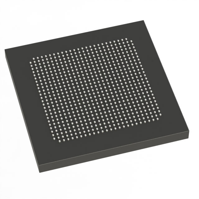
Stratix® V GX Field Programmable Gate Array (FPGA) IC 600 19456000 340000 780-BBGA, FCBGA |
|---|---|
| Quantity | 437 Available (as of June 15, 2026) |

| Product Category | Field Programmable Gate Array (FPGA) |
|---|---|
| Manufacturer | Intel |
| Manufacturing Status | Obsolete |
| Manufacturer Standard Lead Time | Contact Us |
| Datasheet |
Specifications & Environmental
| Device Package | 780-HBGA (33x33) | Grade | Commercial | Operating Temperature | 0°C – 85°C | ||
|---|---|---|---|---|---|---|---|
| Package / Case | 780-BBGA, FCBGA | Number of I/O | 600 | Voltage | 820 mV - 880 mV | ||
| Mounting Method | Surface Mount | RoHS Compliance | RoHS Compliant | REACH Compliance | REACH Unknown | ||
| Moisture Sensitivity Level | 3 (168 Hours) | Number of LABs/CLBs | 128300 | Number of Logic Elements/Cells | 340000 | ||
| Number of Gates | N/A | ECCN | 3A001A2C | HTS Code | 8542.39.0001 | ||
| Qualification | N/A | Total RAM Bits | 19456000 |
Overview of 5SGXMA3E1H29C2L – Stratix® V GX FPGA, 340,000 logic elements, 780‑BBGA
The 5SGXMA3E1H29C2L is a Stratix V GX field-programmable gate array (FPGA) offered in a 780‑ball BGA (FCBGA) package. It provides high-density programmable logic, substantial on-chip memory, and a large I/O count for complex digital designs.
With approximately 340,000 logic elements, about 19.456 Mbits of embedded memory, and 600 I/O pins, this commercial‑grade device is aimed at applications that require extensive logic integration, broad interfacing, and robust on-chip storage while operating within standard commercial temperature conditions.
Key Features
- Core Logic — Approximately 340,000 logic elements for implementing large-scale digital functions and custom accelerators.
- Embedded Memory — Approximately 19.456 Mbits of on-chip RAM to support data buffering, FIFOs, and state storage.
- I/O Capacity — 600 user I/O pins to accommodate high pin-count interfaces and multiple peripheral connections.
- Power and Supply — Core voltage supply range of 820 mV to 880 mV for the device core.
- Package & Mounting — 780‑BBGA, FCBGA package (supplier package: 780‑HBGA, 33×33); surface-mount mounting type suitable for board-level assembly.
- Temperature Grade — Commercial grade with an operating temperature range of 0 °C to 85 °C.
- Standards Compliance — RoHS compliant.
- Stratix V GX Family Characteristics — As a member of the Stratix V GX family, devices in this family are offered with transceiver speed grades described in the series documentation.
Typical Applications
- High‑density digital processing — Implement complex logic, signal processing blocks, and custom compute engines using the large logic‑element count.
- Memory‑intensive designs — Use the device’s approximately 19.456 Mbits of embedded RAM for buffering, packet queues, and intermediate data storage.
- High‑pin-count interfacing — Leverage 600 I/O pins to connect multiple peripherals, buses, or mezzanine modules on a single FPGA.
- Advanced communications and prototyping — Integrate the FPGA into communication systems or development platforms that require flexible, reprogrammable logic and broad I/O availability.
Unique Advantages
- High logic integration: Approximately 340,000 logic elements reduce the need for multiple devices, simplifying system architecture.
- Substantial on‑chip memory: Nearly 19.456 Mbits of embedded RAM supports larger buffering and state retention without external memory.
- Extensive I/O: 600 user I/Os enable dense system integration and flexible interface options for complex boards.
- Board‑level readiness: Surface‑mount 780‑BBGA package (33×33 supplier package) aligns with standard assembly workflows for high‑pin‑count FPGAs.
- Commercial temperature rating: Rated 0 °C to 85 °C for applications targeting commercial environments.
- Regulatory compliance: RoHS compliance supports environmental and manufacturing requirements.
Why Choose 5SGXMA3E1H29C2L?
5SGXMA3E1H29C2L combines large programmable logic capacity, significant embedded memory, and extensive I/O in a single commercial‑grade Stratix V GX FPGA package. It is well suited for designs that demand high integration density, substantial on‑chip storage, and wide interfacing capability while maintaining standard commercial operating characteristics.
For engineering teams and procurement focused on scalable, reprogrammable hardware platforms, this device delivers a balance of logic resources, memory, and I/O that supports complex prototypes, communications subsystems, and dense digital processing applications.
Request a quote or submit an inquiry for 5SGXMA3E1H29C2L to obtain pricing and availability information for your next design.


Date Founded: 1968
Headquarters: Santa Clara, California, USA
Employees: 130,000+
Revenue: $54.23 Billion
Certifications and Memberships: ISO9001:2015, ISO14001:2015, ISO17025:2017, ISO27001:2022, ISO45001:2018, ISO50001:2018


