
5SGXMA3E1H29C2WN
| Part Description |
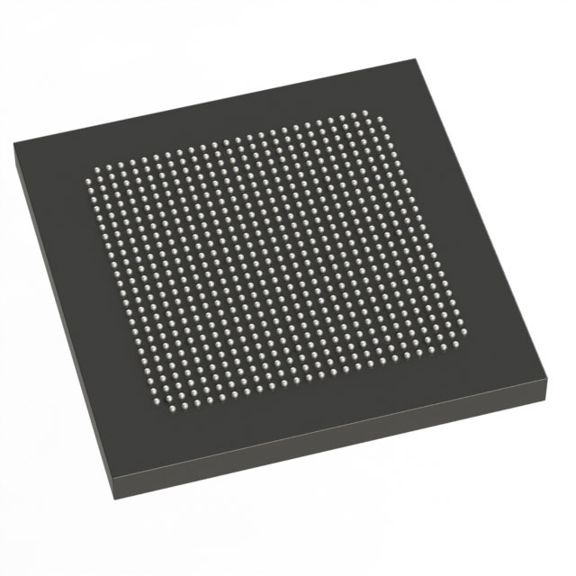
Stratix® V GX Field Programmable Gate Array (FPGA) IC 600 19456000 340000 780-BBGA, FCBGA |
|---|---|
| Quantity | 957 Available (as of June 18, 2026) |

| Product Category | Field Programmable Gate Array (FPGA) |
|---|---|
| Manufacturer | Intel |
| Manufacturing Status | Obsolete |
| Manufacturer Standard Lead Time | Contact Us |
| Datasheet |
Specifications & Environmental
| Device Package | 780-HBGA (33x33) | Grade | Commercial | Operating Temperature | 0°C – 85°C | ||
|---|---|---|---|---|---|---|---|
| Package / Case | 780-BBGA, FCBGA | Number of I/O | 600 | Voltage | 870 mV - 930 mV | ||
| Mounting Method | Surface Mount | RoHS Compliance | RoHS non-compliant | REACH Compliance | REACH Unknown | ||
| Moisture Sensitivity Level | 4 (72 Hours) | Number of LABs/CLBs | 128300 | Number of Logic Elements/Cells | 340000 | ||
| Number of Gates | N/A | ECCN | OBSOLETE | HTS Code | N/A | ||
| Qualification | N/A | Total RAM Bits | 19456000 |
Overview of 5SGXMA3E1H29C2WN – Stratix® V GX Field Programmable Gate Array (FPGA) IC
The 5SGXMA3E1H29C2WN is a Stratix® V GX family FPGA from Intel, implemented in a high-density FCBGA package. It delivers substantial on-chip logic and memory resources together with a large I/O count to address designs that require dense programmable logic and extensive external connectivity.
Key device characteristics include 340,000 logic elements, approximately 19.456 Mbits of embedded memory, 600 I/Os, and a low-voltage core operating range of 870 mV–930 mV. The device is offered in a commercial temperature grade (0 °C to 85 °C) and is RoHS compliant.
Key Features
- Core Architecture Stratix V GX family FPGA architecture implemented in this part number, providing large-scale programmable logic capacity.
- Logic Capacity 340,000 logic elements to support complex combinational and sequential logic designs.
- Embedded Memory Approximately 19.456 Mbits of on-chip RAM for buffering, lookup tables, and state storage.
- I/O Density 600 I/O pins to support wide parallel interfaces, multi-channel connectivity, and high-pin-count designs.
- Power and Core Voltage Core supply range of 870 mV–930 mV to match system power rails and optimize core operation.
- Package and Mounting 780-ball BGA (FCBGA) package; supplier device package listed as 780-HBGA (33×33). Surface-mount mounting type.
- Operating Conditions Commercial temperature grade with an operating range of 0 °C to 85 °C.
- Environmental Compliance RoHS compliant.
Typical Applications
- High-density digital systems Implement large-scale logic functions and complex state machines using the device's 340,000 logic elements and embedded RAM.
- Data buffering and packet processing Leverage approximately 19.456 Mbits of on-chip memory and 600 I/Os for multi-channel buffering and parallel data paths.
- High-pin-count interface hubs Use the 600 I/O pins in FCBGA packaging to aggregate and route signals across dense connector or mezzanine designs.
Unique Advantages
- High logic density: 340,000 logic elements provide the capacity needed for substantial programmable logic integration within a single device.
- Significant embedded memory: Approximately 19.456 Mbits of on-chip RAM reduces dependence on external memory for many buffering and LUT applications.
- Extensive I/O capability: 600 I/Os support complex, parallel interfaces and multiple external subsystems without immediate need for additional glue logic.
- Compact BGA package: 780-ball FCBGA in a 33×33 supplier footprint enables a high-pin-count implementation in a single-socket footprint for compact board layouts.
- Low-voltage core operation: Core supply range of 870 mV–930 mV supports modern low-voltage system architectures.
- Commercial-grade availability: Rated for 0 °C to 85 °C operation and RoHS compliant for standard commercial applications.
Why Choose 5SGXMA3E1H29C2WN?
The 5SGXMA3E1H29C2WN combines large logic capacity, substantial on-chip memory, and a high I/O count in a single FCBGA package—making it suitable for designs that require dense integration of programmable logic and wide external interfacing. As a Stratix V GX device from Intel, it provides a clear specification set for teams targeting commercial-temperature applications with defined core-voltage requirements.
Choose this part when your design needs a single-chip solution for heavy logic workloads, significant embedded RAM, and broad I/O connectivity while maintaining a compact board footprint and RoHS compliance.
Request a quote or submit a purchase inquiry to receive pricing and availability for the 5SGXMA3E1H29C2WN.


Date Founded: 1968
Headquarters: Santa Clara, California, USA
Employees: 130,000+
Revenue: $54.23 Billion
Certifications and Memberships: ISO9001:2015, ISO14001:2015, ISO17025:2017, ISO27001:2022, ISO45001:2018, ISO50001:2018


