
5SGXMA3E1H29I2G
| Part Description |
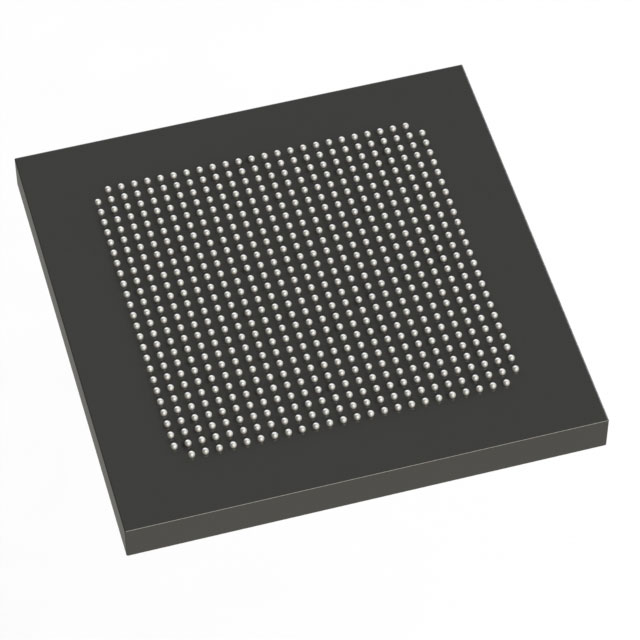
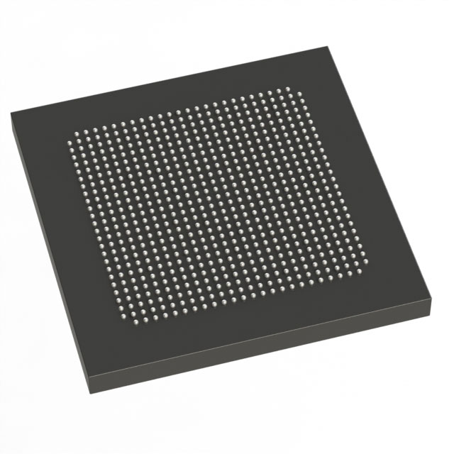
Stratix® V GX Field Programmable Gate Array (FPGA) IC 600 19456000 340000 780-BBGA, FCBGA |
|---|---|
| Quantity | 186 Available (as of October 8, 2026) |
| Product Category | Field Programmable Gate Array (FPGA) |
|---|---|
| Manufacturer | Intel |
| Manufacturing Status | Active |
| Manufacturer Standard Lead Time | 26 Weeks |
| Datasheet |
Specifications & Environmental
| Device Package | 780-HBGA (33x33) | Grade | Industrial | Operating Temperature | -40°C – 100°C | ||
|---|---|---|---|---|---|---|---|
| Package / Case | 780-BBGA, FCBGA | Number of I/O | 600 | Voltage | 870 mV - 930 mV | ||
| Mounting Method | Surface Mount | RoHS Compliance | RoHS Compliant | REACH Compliance | REACH Unaffected | ||
| Moisture Sensitivity Level | 3 (168 Hours) | Number of LABs/CLBs | 128300 | Number of Logic Elements/Cells | 340000 | ||
| Number of Gates | N/A | ECCN | N/A | HTS Code | N/A | ||
| Qualification | N/A | Total RAM Bits | 19456000 |
Overview of 5SGXMA3E1H29I2G – Stratix® V GX FPGA, 340000 logic elements
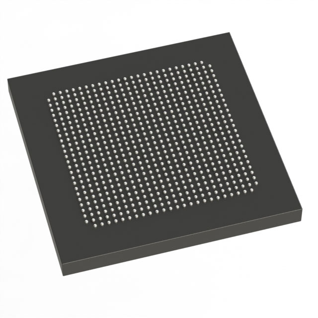
The 5SGXMA3E1H29I2G is an Intel Stratix® V GX field programmable gate array (FPGA) in a 780‑ball FCBGA package, offered as an industrial‑grade device. It delivers large programmable logic capacity combined with substantial on‑chip memory and a high I/O count for demanding embedded and industrial systems.
Built for applications that require high logic density, ample embedded RAM, and robust board‑level integration, this device supports designs that need up to 600 I/O pins, operation across a wide temperature range, and core supply operation within a low‑voltage domain.
Key Features
- Logic Capacity 340,000 logic elements provide extensive programmable fabric for complex digital designs.
- Embedded Memory Approximately 19.456 Mbits of on‑chip RAM to support large buffers, FIFOs, and cache‑style structures.
- I/O Density Up to 600 user I/O pins to support wide parallel interfaces and numerous peripheral connections.
- Core Voltage Core supply range of 870 mV to 930 mV for the device core power domain.
- Industrial Temperature Grade Rated for operation from −40 °C to 100 °C for applications requiring extended temperature tolerance.
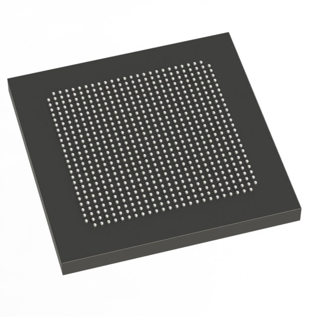
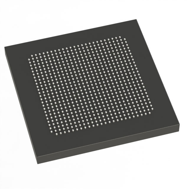
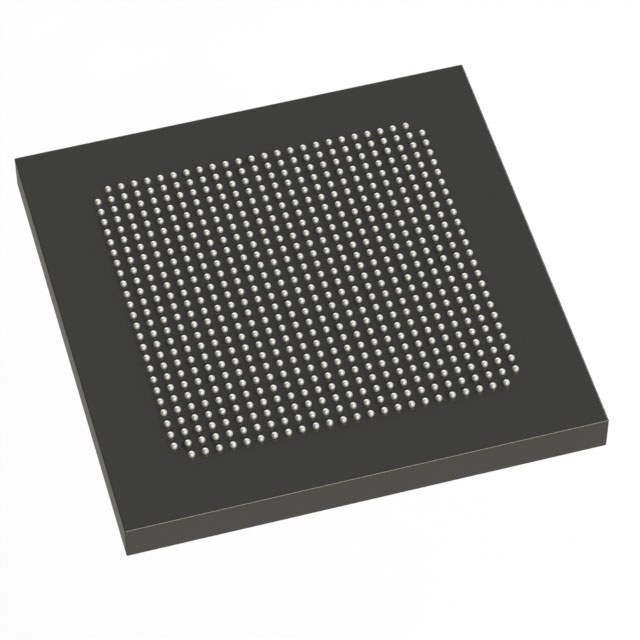
- Package and Mounting 780‑ball BBGA (FCBGA) package; supplier package noted as 780‑HBGA (33×33), surface‑mount mounting type.
- Standards and Compliance RoHS compliant to meet environmental and manufacturing requirements.
- Series Transceiver Options (Series-level) The Stratix V family documentation lists GX transceiver speed grades including channel options up to 14.1 Gbps (series datasheet information).
Typical Applications
- High‑density digital processing Implement complex custom logic, signal processing pipelines, and protocol engines using the 340,000 logic elements and large embedded RAM.
- Multi‑interface systems Support wide arrays of peripherals and parallel interfaces with up to 600 I/O pins.
- Industrial equipment and controls Deploy in systems requiring robust thermal performance and an extended operating temperature range (−40 °C to 100 °C).
- Board‑level integration Use the 780‑ball FCBGA package for compact, surface‑mount implementations that consolidate logic and memory on a single device.
Unique Advantages
- Substantial programmable capacity: 340,000 logic elements enable large, integrated designs that reduce external components.
- Significant on‑chip RAM: Approximately 19.456 Mbits of embedded memory simplifies data buffering and reduces reliance on external memory.
- High I/O availability: 600 I/O pins give designers flexibility to connect multiple interfaces and sensors directly to the FPGA.
- Industrial thermal range: Operation from −40 °C to 100 °C supports deployment in temperature‑challenging environments.
- Low‑voltage core: Core supply specified between 870 mV and 930 mV to align with low‑voltage power domains on modern boards.
- Regulatory and assembly readiness: RoHS compliance and a surface‑mount FCBGA package streamline manufacturing and environmental compliance.
Why Choose 5SGXMA3E1H29I2G?
The 5SGXMA3E1H29I2G positions itself as a high‑capacity Stratix V GX FPGA option for designers who need a large logic fabric, substantial embedded memory, and a high I/O count in an industrial‑rated device. Its package and mounting format support compact board layouts while delivering the resources required to consolidate complex functions into a single FPGA.
This part is appropriate for engineering teams building industrial systems, high‑density digital platforms, or multi‑interface solutions that demand extended temperature operation and RoHS compliance. The combination of logic capacity, on‑chip RAM, and I/O resources offers long‑term design scalability and robustness within the Stratix V family.
Request a quote or submit an inquiry to receive pricing, availability, and technical purchasing information for the 5SGXMA3E1H29I2G. Provide your project requirements and quantity to get a tailored response.





















Date Founded: 1968
Headquarters: Santa Clara, California, USA
Employees: 130,000+
Revenue: $54.23 Billion
Certifications and Memberships: ISO9001:2015, ISO14001:2015, ISO17025:2017, ISO27001:2022, ISO45001:2018, ISO50001:2018


