
5SGXMA3E2H29C1N
| Part Description |
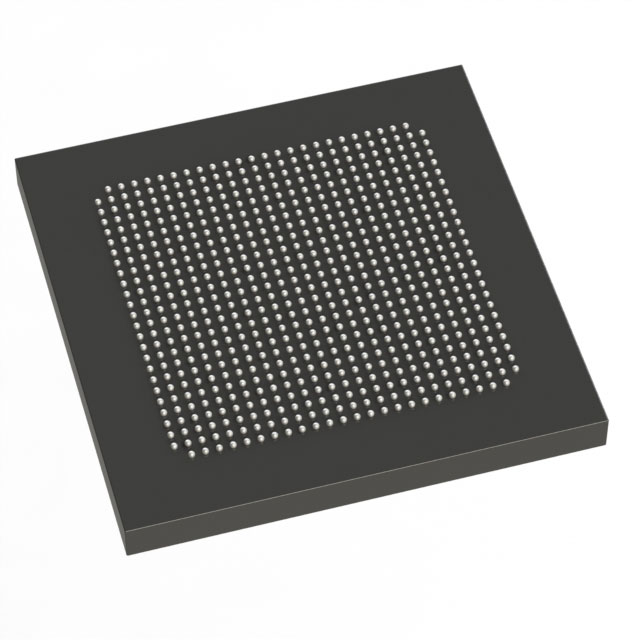
Stratix® V GX Field Programmable Gate Array (FPGA) IC 600 19456000 340000 780-BBGA, FCBGA |
|---|---|
| Quantity | 1,317 Available (as of June 18, 2026) |
| Product Category | Field Programmable Gate Array (FPGA) |
|---|---|
| Manufacturer | Intel |
| Manufacturing Status | Obsolete |
| Manufacturer Standard Lead Time | Contact Us |
| Datasheet |
Specifications & Environmental
| Device Package | 780-HBGA (33x33) | Grade | Commercial | Operating Temperature | 0°C – 85°C | ||
|---|---|---|---|---|---|---|---|
| Package / Case | 780-BBGA, FCBGA | Number of I/O | 600 | Voltage | 870 mV - 930 mV | ||
| Mounting Method | Surface Mount | RoHS Compliance | RoHS Compliant | REACH Compliance | REACH Unknown | ||
| Moisture Sensitivity Level | 3 (168 Hours) | Number of LABs/CLBs | 128300 | Number of Logic Elements/Cells | 340000 | ||
| Number of Gates | N/A | ECCN | 3A001A2C | HTS Code | 8542.39.0001 | ||
| Qualification | N/A | Total RAM Bits | 19456000 |
Overview of 5SGXMA3E2H29C1N – Stratix® V GX FPGA, 340,000 logic elements
The 5SGXMA3E2H29C1N is an Intel Stratix® V GX field-programmable gate array (FPGA) in a 780-ball BGA (FCBGA) package. It delivers large programmable logic capacity, extensive embedded memory, and a high pin count to support complex, high-density digital designs.
Built for commercial-grade applications, this device combines 340,000 logic elements, approximately 19.5 Mbits of on-chip RAM, and 600 I/O pins to address demanding workloads that require significant logic, memory, and I/O integration while operating from a 0°C to 85°C temperature range and a core voltage between 870 mV and 930 mV.
Key Features
- Logic Capacity — 340,000 logic elements and 128,300 logic array blocks provide substantial programmable fabric for large-scale designs.
- Embedded Memory — Approximately 19.5 Mbits of total on-chip RAM to support large buffering, lookup tables, and state storage.
- I/O Resources — 600 I/O pins to accommodate high connector counts, multi-channel interfaces, and extensive peripheral connectivity.
- Power and Voltage — Core voltage supply specified at 870 mV to 930 mV for defined power and timing behavior.
- Package & Mounting — 780-BBGA (supplier package listed as 780-HBGA, 33×33) in an FCBGA form factor; surface-mount for PCB integration.
- Operating Grade & Temperature — Commercial grade with an operating temperature range of 0°C to 85°C.
- Standards Compliance — RoHS compliant.
- Stratix V GX Family Characteristics — As a member of the Stratix V GX family, the device is documented in the Stratix V device datasheet covering electrical and switching characteristics, I/O timing, and transceiver/periphery performance.
Typical Applications
- High‑density digital processing — Use the large logic capacity and embedded memory for complex FPGA-based compute pipelines and algorithm implementation.
- Multi‑channel I/O systems — 600 I/O pins support boards requiring many external interfaces, sensors, or multi-lane connectivity.
- Data buffering and packet processing — Significant on-chip RAM provides space for queues, FIFOs, and packet-handling logic.
Unique Advantages
- Large programmable fabric: 340,000 logic elements enable implementation of highly parallel designs and large custom accelerators.
- Substantial embedded memory: Approximately 19.5 Mbits of RAM reduces dependence on external memory for many buffering and storage needs.
- High I/O density: 600 I/O pins simplify designs that require many external connections without needing additional interface chips.
- Commercial-grade suitability: Specified for 0°C to 85°C operation to match typical commercial environmental requirements.
- Defined power envelope: Core supply range of 870 mV–930 mV allows predictable power and timing design margining.
- Surface-mount BGA packaging: 780-ball FCBGA (33×33) package supports compact, high-density PCB layouts.
Why Choose 5SGXMA3E2H29C1N?
This Stratix V GX FPGA offers a compelling combination of large logic capacity, ample embedded memory, and high I/O count in a commercial-grade FCBGA package. It is suited to designers who need to integrate complex digital functions, substantial buffering, and many external interfaces on a single programmable device while keeping to defined voltage and temperature requirements.
The device is supported by the Stratix V device documentation for electrical and switching characteristics, enabling informed system-level power and timing design. Its packaging and RoHS compliance simplify board-level integration for commercial applications that require dense, high-capacity FPGA resources.
Request a quote or submit an inquiry to discuss availability, lead times, and pricing for the 5SGXMA3E2H29C1N.


Date Founded: 1968
Headquarters: Santa Clara, California, USA
Employees: 130,000+
Revenue: $54.23 Billion
Certifications and Memberships: ISO9001:2015, ISO14001:2015, ISO17025:2017, ISO27001:2022, ISO45001:2018, ISO50001:2018


