
5SGXMA3E2H29C2G
| Part Description |
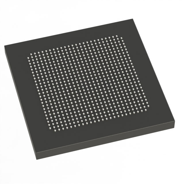
Stratix® V GX Field Programmable Gate Array (FPGA) IC 600 19456000 340000 780-BBGA, FCBGA |
|---|---|
| Quantity | 1,066 Available (as of June 15, 2026) |

| Product Category | Field Programmable Gate Array (FPGA) |
|---|---|
| Manufacturer | Intel |
| Manufacturing Status | Active |
| Manufacturer Standard Lead Time | 26 Weeks |
| Datasheet |
Specifications & Environmental
| Device Package | 780-HBGA (33x33) | Grade | Commercial | Operating Temperature | 0°C – 85°C | ||
|---|---|---|---|---|---|---|---|
| Package / Case | 780-BBGA, FCBGA | Number of I/O | 600 | Voltage | 870 mV - 930 mV | ||
| Mounting Method | Surface Mount | RoHS Compliance | RoHS Compliant | REACH Compliance | REACH Unaffected | ||
| Moisture Sensitivity Level | 3 (168 Hours) | Number of LABs/CLBs | 128300 | Number of Logic Elements/Cells | 340000 | ||
| Number of Gates | N/A | ECCN | N/A | HTS Code | N/A | ||
| Qualification | N/A | Total RAM Bits | 19456000 |
Overview of 5SGXMA3E2H29C2G – Stratix® V GX FPGA, 340,000 logic elements
The 5SGXMA3E2H29C2G is a Stratix V GX field-programmable gate array (FPGA) IC delivering high logic density and extensive on-chip memory for complex digital designs. As a GX-class Stratix V device, it is part of a family that includes high-speed transceiver capability and comprehensive I/O resources, addressing designs that require large programmable logic arrays and substantial embedded RAM.
Engineered for commercial-temperature applications, this device combines 340,000 logic elements, approximately 19.456 Mbits of embedded memory, and 600 I/O pins in a 780-ball BGA package to support data-processing, multi-channel I/O, and high-density integration requirements.
Key Features
- Logic Capacity 340,000 logic elements to implement large-scale digital logic and complex state machines.
- Embedded Memory Approximately 19.456 Mbits of on-chip RAM for buffering, LUT-based storage, and data-path implementations.
- I/O Resources 600 I/O pins to support wide parallel interfaces and multi-channel connectivity.
- Transceiver Capability (Series-Level) Stratix V GX devices support high-speed transceiver speed grades (series documentation lists GX channel options up to 14.1 Gbps), suitable for high-speed serial link implementations.
- Power and Core Voltage Core voltage supply range from 870 mV to 930 mV, enabling operation at the device’s specified core levels.
- Package 780-ball BGA (FCBGA / supplier 780-HBGA, 33 × 33 mm) for high-density board-level mounting and thermal/mechanical stability.
- Operating Conditions Commercial grade operation with an ambient temperature range of 0 °C to 85 °C.
- RoHS Compliance Device is RoHS compliant.
Typical Applications
- High-speed serial interfaces Leverage the Stratix V GX transceiver speed-grade support and 600 I/Os for multi-lane serial links and backplane connectivity.
- High-density logic and compute Deploy the 340,000 logic elements and ~19.456 Mbits of embedded RAM for complex signal processing, packet processing, and custom compute accelerators.
- Data aggregation and buffering Use the large on-chip RAM and abundant I/Os for data buffering, interface bridging, and multi-protocol aggregation tasks.
Unique Advantages
- High logic density: 340,000 logic elements enable implementation of large, integrated designs without external programmable logic.
- Substantial embedded memory: Approximately 19.456 Mbits of on-chip RAM reduces dependence on external memory for many buffering and data-path requirements.
- Extensive I/O count: 600 I/Os provide flexibility for wide parallel buses, multiple interfaces, and channel-rich applications.
- Commercial-grade operating range: Rated for 0 °C to 85 °C to match standard commercial deployments and system environments.
- High-density BGA package: 780-ball FCBGA (33 × 33 mm) supports compact board layouts and robust electrical performance.
Why Choose 5SGXMA3E2H29C2G?
The 5SGXMA3E2H29C2G balances very high logic capacity and on-chip memory with a large I/O complement, making it well-suited for designs that require dense programmable logic, significant embedded RAM, and multi-channel connectivity. Its Stratix V GX lineage provides access to series-level transceiver capabilities and detailed device electrical and timing characteristics for rigorous system design.
This device targets engineers and system architects building high-performance communication, data-processing, or integration-heavy designs who need a commercially rated FPGA with proven series-level specifications and a high degree of functional integration.
Request a quote or submit an RFQ to get pricing and availability for the 5SGXMA3E2H29C2G. Provide your requirements and quantities to receive a prompt response.


Date Founded: 1968
Headquarters: Santa Clara, California, USA
Employees: 130,000+
Revenue: $54.23 Billion
Certifications and Memberships: ISO9001:2015, ISO14001:2015, ISO17025:2017, ISO27001:2022, ISO45001:2018, ISO50001:2018


