
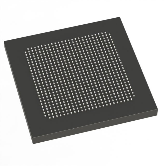
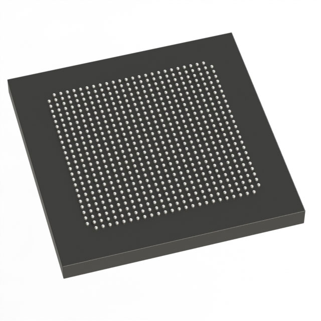
5SGXMA3E2H29C3G
| Part Description |
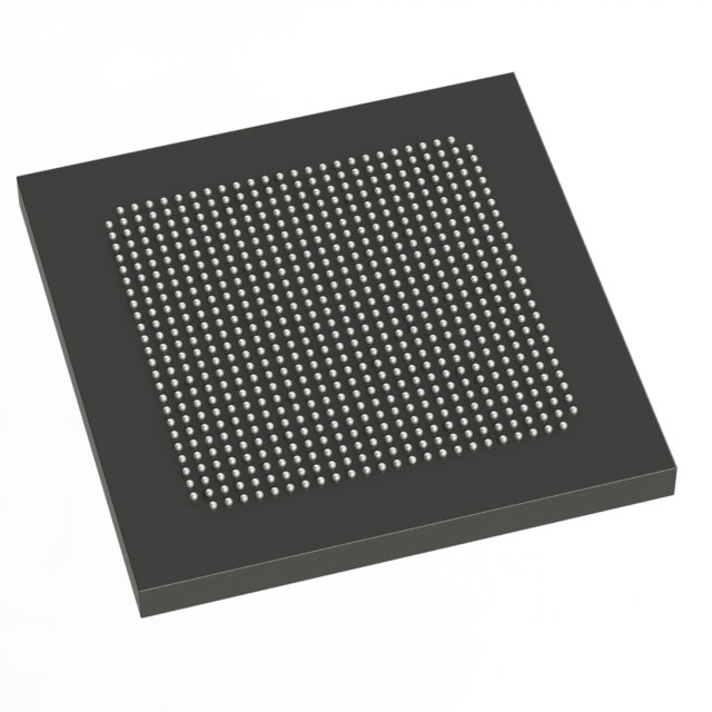
Stratix® V GX Field Programmable Gate Array (FPGA) IC 600 19456000 340000 780-BBGA, FCBGA |
|---|---|
| Quantity | 526 Available (as of October 7, 2026) |
| Product Category | Field Programmable Gate Array (FPGA) |
|---|---|
| Manufacturer | Intel |
| Manufacturing Status | Active |
| Manufacturer Standard Lead Time | 26 Weeks |
| Datasheet |
Specifications & Environmental
| Device Package | 780-HBGA (33x33) | Grade | Commercial | Operating Temperature | 0°C – 85°C | ||
|---|---|---|---|---|---|---|---|
| Package / Case | 780-BBGA, FCBGA | Number of I/O | 600 | Voltage | 820 mV - 880 mV | ||
| Mounting Method | Surface Mount | RoHS Compliance | RoHS Compliant | REACH Compliance | REACH Unaffected | ||
| Moisture Sensitivity Level | 3 (168 Hours) | Number of LABs/CLBs | 128300 | Number of Logic Elements/Cells | 340000 | ||
| Number of Gates | N/A | ECCN | N/A | HTS Code | N/A | ||
| Qualification | N/A | Total RAM Bits | 19456000 |
Overview of 5SGXMA3E2H29C3G – Stratix® V GX Field Programmable Gate Array (FPGA) IC
The 5SGXMA3E2H29C3G is a Stratix V GX family FPGA IC offering high-density programmable logic, on-chip embedded memory, and a large I/O complement in a 780‑ball BGA package. It delivers 340,000 logic elements and approximately 19.456 Mbits of embedded memory, with up to 600 user I/Os for complex, I/O‑heavy designs.
Designed as a commercial‑grade device, this surface‑mount FCBGA (780‑BBGA / supplier package 780‑HBGA, 33×33) targets applications that require significant programmable resources and multi‑gigabit transceiver capability as described in the Stratix V device datasheet.
Key Features
- Core Logic 340,000 logic elements to implement large digital functions and system logic.
- Embedded Memory Approximately 19.456 Mbits of on‑chip RAM for buffering, LUTRAM, and system state storage.
- I/O Capacity Up to 600 user I/Os to support wide data buses, numerous peripherals, and complex board-level interconnect.
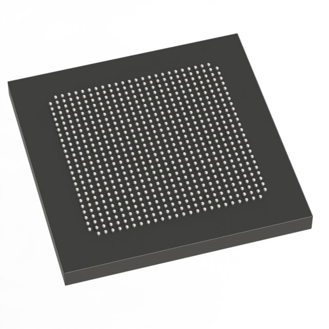
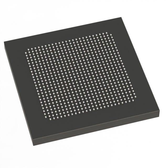
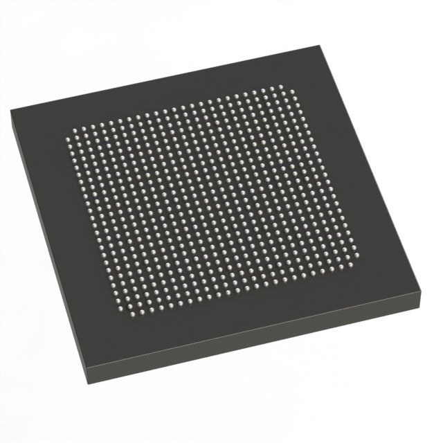
- Package & Mounting 780‑BBGA FCBGA package (supplier device package: 780‑HBGA, 33×33) with surface mount construction for compact, high-density PCB designs.
- Power Core voltage supply range of 820 mV to 880 mV, enabling specified operating conditions for the device core.
- Operating Conditions & Grade Commercial temperature grade with an operating range of 0 °C to 85 °C.
- Compliance RoHS compliant to meet current environmental directives.
- Family Documentation The Stratix V device datasheet provides detailed information on transceiver speed grades, electrical characteristics, and device operating requirements.
Typical Applications
- High‑Speed Communications Leverages Stratix V GX transceiver capabilities (documented in the family datasheet) for multi‑gigabit links and protocol handling.
- Networking & Data Path Acceleration High logic density and large embedded RAM make the device suitable for packet processing, switching, and data acceleration functions.
- Signal Processing & DSP On‑chip memory and abundant logic elements support real‑time signal processing pipelines and algorithmic implementations.
- Complex System Prototyping Large I/O count and reprogrammable logic enable integration of multiple subsystems and rapid iteration during development.
Unique Advantages
- High programmable density: 340,000 logic elements provide the capacity to implement large, consolidated logic designs and complex state machines.
- Substantial embedded memory: Approximately 19.456 Mbits of on‑chip RAM reduces external memory dependency and improves data throughput.
- Extensive I/O resources: 600 I/Os simplify board routing for multi‑channel interfaces and parallel data paths.
- Compact, manufacturable package: 780‑ball BGA (33×33) surface‑mount package supports high‑density PCB assembly and reliable solder mounting.
- Commercial availability and compliance: Commercial temperature grade operation and RoHS compliance support mainstream production deployments.
- Documented family capabilities: The Stratix V datasheet provides detailed electrical, switching, and transceiver specifications to guide system integration and validation.
Why Choose 5SGXMA3E2H29C3G?
The 5SGXMA3E2H29C3G positions itself as a high‑density, commercial‑grade Stratix V GX FPGA that balances large programmable logic capacity, on‑chip memory, and extensive I/O in a compact BGA footprint. It is well suited for engineering teams designing high‑performance communications, networking, and signal processing systems that require significant internal resources and documented transceiver capabilities.
With regulated core voltage requirements and family‑level datasheet coverage for electrical and transceiver behavior, this device supports disciplined system design, scalability across Stratix V options, and integration into production workflows where commercial temperature operation and RoHS compliance are required.
Request a quote or submit an inquiry to obtain pricing, availability, and further technical assistance for 5SGXMA3E2H29C3G.





















Date Founded: 1968
Headquarters: Santa Clara, California, USA
Employees: 130,000+
Revenue: $54.23 Billion
Certifications and Memberships: ISO9001:2015, ISO14001:2015, ISO17025:2017, ISO27001:2022, ISO45001:2018, ISO50001:2018


