
5SGXMA3E3H29C3G
| Part Description |
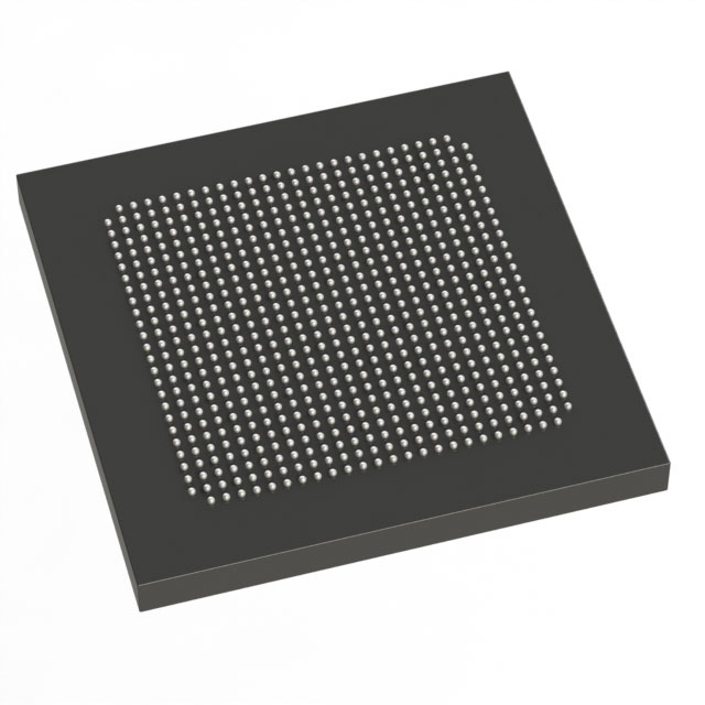
Stratix® V GX Field Programmable Gate Array (FPGA) IC 600 19456000 340000 780-BBGA, FCBGA |
|---|---|
| Quantity | 409 Available (as of June 17, 2026) |

| Product Category | Field Programmable Gate Array (FPGA) |
|---|---|
| Manufacturer | Intel |
| Manufacturing Status | Active |
| Manufacturer Standard Lead Time | 26 Weeks |
| Datasheet |
Specifications & Environmental
| Device Package | 780-HBGA (33x33) | Grade | Commercial | Operating Temperature | 0°C – 85°C | ||
|---|---|---|---|---|---|---|---|
| Package / Case | 780-BBGA, FCBGA | Number of I/O | 600 | Voltage | 820 mV - 880 mV | ||
| Mounting Method | Surface Mount | RoHS Compliance | RoHS Compliant | REACH Compliance | REACH Unaffected | ||
| Moisture Sensitivity Level | 3 (168 Hours) | Number of LABs/CLBs | 128300 | Number of Logic Elements/Cells | 340000 | ||
| Number of Gates | N/A | ECCN | N/A | HTS Code | N/A | ||
| Qualification | N/A | Total RAM Bits | 19456000 |
Overview of 5SGXMA3E3H29C3G – Stratix® V GX Field Programmable Gate Array (FPGA) IC 600 19456000 340000 780-BBGA, FCBGA
The 5SGXMA3E3H29C3G is a Stratix V GX Field Programmable Gate Array (FPGA) provided in a 780‑BBGA FCBGA package. It delivers high logic capacity and on‑chip memory suitable for complex digital designs requiring extensive I/O and embedded RAM.
Key device attributes include 340,000 logic elements, approximately 19.456 Mbits of embedded memory, 600 I/O pins, a supply voltage range of 820–880 mV, and a commercial operating temperature range of 0 °C to 85 °C. The device is RoHS compliant and supplied as a surface‑mount FCBGA package (780‑HBGA, 33×33).
Key Features
- Core Logic Capacity 340,000 logic elements for implementing large-scale combinational and sequential logic networks.
- Embedded Memory Approximately 19.456 Mbits of on‑chip RAM to support buffering, lookup tables, and state storage within the FPGA fabric.
- I/O Resources 600 I/O pins to accommodate extensive peripheral interfacing and multi‑lane connectivity requirements.
- Power Supply Core supply voltage range of 820 mV to 880 mV, enabling designs that target the specified core operating conditions.
- Package and Mounting 780‑BBGA FCBGA package (supplier package: 780‑HBGA, 33×33) in a surface‑mount form factor for high‑density PCB integration.
- Operating Grade and Temperature Commercial grade device with an operating temperature range of 0 °C to 85 °C.
- RoHS Compliant Device material and assembly conform to RoHS requirements.
- Family Transceiver Capability (series-level) The Stratix V GX family documentation lists transceiver speed grades including up to 14.1 Gbps (family-level data referenced from the Stratix V device datasheet).
Typical Applications
- High‑density digital processing Large logic capacity and embedded RAM enable implementation of complex datapaths, state machines, and custom accelerators.
- Multi‑lane I/O systems 600 I/O pins support extensive parallel and serial interfacing for board‑level connectivity and multi‑interface designs.
- On‑chip buffering and memory‑intensive logic Approximately 19.456 Mbits of embedded memory for packet buffering, LUTs, and temporary data storage within FPGA fabric.
Unique Advantages
- High logic density: 340,000 logic elements reduce reliance on external logic devices for complex implementations.
- Significant on‑chip memory: Approximately 19.456 Mbits of embedded RAM enables efficient local data handling and state retention.
- Extensive I/O count: 600 I/O pins provide flexibility for multiple peripherals, parallel buses, and high-pin‑count interfaces.
- Commercial temperature grade: Rated for 0 °C to 85 °C operation for a wide range of standard commercial applications.
- Robust package option: 780‑BBGA FCBGA (780‑HBGA, 33×33) surface‑mount package supports high‑density PCB assembly.
- Standards‑aware family characteristics: Stratix V GX family documentation includes high‑speed transceiver speed grades (family-level reference), useful when evaluating system‑level connectivity requirements.
Why Choose 5SGXMA3E3H29C3G?
The 5SGXMA3E3H29C3G combines large programmable logic capacity, substantial embedded memory, and a high I/O count in a commercial‑grade surface‑mount FCBGA package. These characteristics make it suitable for designers who need substantial on‑chip resources and flexible interfacing in board‑level FPGA implementations.
Choosing this Stratix V GX device supports scalable, high‑density designs where integrated RAM and extensive I/O reduce external component count and simplify system architecture. The device benefits from documented family‑level electrical and transceiver characteristics in the Stratix V datasheet for design planning and validation.
Request a quote or submit your inquiry to start the procurement process for the 5SGXMA3E3H29C3G and get component availability and pricing information for your next design.


Date Founded: 1968
Headquarters: Santa Clara, California, USA
Employees: 130,000+
Revenue: $54.23 Billion
Certifications and Memberships: ISO9001:2015, ISO14001:2015, ISO17025:2017, ISO27001:2022, ISO45001:2018, ISO50001:2018


