
5SGXMA3K3F35I3N
| Part Description |
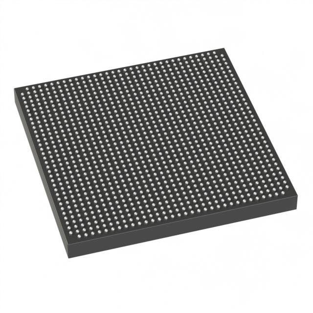
Stratix® V GX Field Programmable Gate Array (FPGA) IC 600 19456000 340000 1152-BBGA, FCBGA |
|---|---|
| Quantity | 371 Available (as of June 10, 2026) |
| Product Category | Field Programmable Gate Array (FPGA) |
|---|---|
| Manufacturer | Intel |
| Manufacturing Status | Obsolete |
| Manufacturer Standard Lead Time | Contact Us |
| Datasheet |
Specifications & Environmental
| Device Package | 1152-FBGA (35x35) | Grade | Industrial | Operating Temperature | -40°C – 100°C | ||
|---|---|---|---|---|---|---|---|
| Package / Case | 1152-BBGA, FCBGA | Number of I/O | 600 | Voltage | 820 mV - 880 mV | ||
| Mounting Method | Surface Mount | RoHS Compliance | RoHS Compliant | REACH Compliance | REACH Unknown | ||
| Moisture Sensitivity Level | 3 (168 Hours) | Number of LABs/CLBs | 128300 | Number of Logic Elements/Cells | 340000 | ||
| Number of Gates | N/A | ECCN | 3A001A2C | HTS Code | 8542.39.0001 | ||
| Qualification | N/A | Total RAM Bits | 19456000 |
Overview of 5SGXMA3K3F35I3N – Stratix® V GX Field Programmable Gate Array (FPGA) IC
The 5SGXMA3K3F35I3N is a Stratix V GX family FPGA in a 1152‑ball FCBGA package, designed for high-density programmable logic implementations. This device combines 340,000 logic elements with approximately 19.46 Mbits of on‑chip RAM and up to 600 I/O pins to address complex, I/O‑rich designs.
Electrical and switching characteristics for the Stratix V family — including operating conditions and power — are documented in the device datasheet for design and system integration reference.
Key Features
- Core Logic Density Approximately 340,000 logic elements provide large on‑chip programmable logic capacity for complex algorithms and parallel processing.
- Embedded Memory Approximately 19.46 Mbits of embedded RAM for buffering, FIFOs, and data‑path storage within the FPGA fabric.
- I/O Capability Up to 600 user I/O pins support dense external connectivity and multiple peripheral interfaces.
- Package 1152‑BBGA (FCBGA) package; supplier device package listed as 1152‑FBGA (35×35) for compact, high‑pin‑count board integration.
- Low‑Voltage Core Core supply range of 820 mV to 880 mV to match low‑voltage FPGA core domains.
- Operating Temperature Industrial temperature grade with rated operation from −40 °C to 100 °C for deployment in thermally demanding environments.
- Mounting Surface‑mount package suitable for modern PCB assembly flows.
- RoHS Compliance Device is RoHS compliant.
Typical Applications
- High‑density logic designs Systems that require substantial programmable logic and on‑chip memory capacity, leveraging the device's 340,000 logic elements and ~19.46 Mbits of RAM.
- I/O‑intensive systems Applications needing extensive external connectivity can utilize the device's up to 600 I/O pins for parallel interfaces and multiple peripherals.
- Industrial temperature deployments Equipment operating across a wide temperature range can benefit from the device's −40 °C to 100 °C rating.
Unique Advantages
- High programmable capacity: 340,000 logic elements enable partitioning of complex functions into a single device, reducing cross‑device interconnect complexity.
- Substantial embedded memory: Approximately 19.46 Mbits of on‑chip RAM supports large buffering and on‑chip data storage without immediate external memory dependence.
- Large I/O count: Up to 600 I/O pins simplify board routing for multi‑interface designs and reduce the need for external I/O expanders.
- Compact, high‑pin package: The 1152‑ball FCBGA footprint delivers high pin density for space‑constrained PCBs while maintaining signal routing options.
- Industrial temperature rating: Designed for reliable operation across −40 °C to 100 °C, supporting deployments in harsher thermal environments.
- Documented electrical/switching characteristics: Stratix V family datasheet provides the device electrical and switching parameters necessary for system design and power budgeting.
Why Choose 5SGXMA3K3F35I3N?
The 5SGXMA3K3F35I3N positions itself as a high‑density Stratix V GX FPGA option for designers who need extensive logic resources, substantial on‑chip RAM, and a high I/O count in a compact FCBGA package. Its industrial temperature rating and documented electrical characteristics make it suitable for demanding embedded and board‑level designs that must manage power, I/O capacity, and thermal constraints.
This device is appropriate for engineering teams seeking a scalable, high‑capacity FPGA building block where on‑chip memory, logic density, and I/O availability are key selection criteria.
Request a quote or submit an RFQ to receive pricing and availability for the 5SGXMA3K3F35I3N. Provide your part number and quantity requirements to start the procurement process.


Date Founded: 1968
Headquarters: Santa Clara, California, USA
Employees: 130,000+
Revenue: $54.23 Billion
Certifications and Memberships: ISO9001:2015, ISO14001:2015, ISO17025:2017, ISO27001:2022, ISO45001:2018, ISO50001:2018


