
5SGXMA5H1F35C2WN
| Part Description |
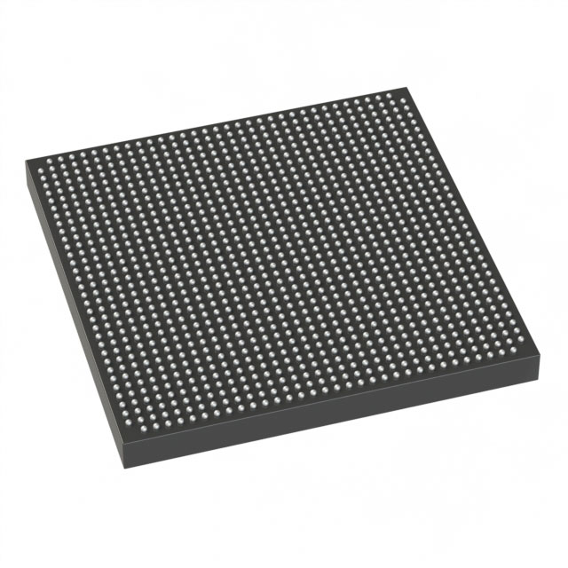
Stratix® V GX Field Programmable Gate Array (FPGA) IC 552 46080000 490000 1152-BBGA, FCBGA |
|---|---|
| Quantity | 1,496 Available (as of June 18, 2026) |

| Product Category | Field Programmable Gate Array (FPGA) |
|---|---|
| Manufacturer | Intel |
| Manufacturing Status | Obsolete |
| Manufacturer Standard Lead Time | Contact Us |
| Datasheet |
Specifications & Environmental
| Device Package | 1152-FBGA (35x35) | Grade | Commercial | Operating Temperature | 0°C – 85°C | ||
|---|---|---|---|---|---|---|---|
| Package / Case | 1152-BBGA, FCBGA | Number of I/O | 552 | Voltage | 870 mV - 930 mV | ||
| Mounting Method | Surface Mount | RoHS Compliance | RoHS non-compliant | REACH Compliance | REACH Unknown | ||
| Moisture Sensitivity Level | 4 (72 Hours) | Number of LABs/CLBs | 185000 | Number of Logic Elements/Cells | 490000 | ||
| Number of Gates | N/A | ECCN | OBSOLETE | HTS Code | N/A | ||
| Qualification | N/A | Total RAM Bits | 46080000 |
Overview of 5SGXMA5H1F35C2WN – Stratix® V GX FPGA, 490,000 logic elements, ~46 Mbits RAM, 552 I/O, 1152‑BBGA
The 5SGXMA5H1F35C2WN is a Stratix V GX field programmable gate array (FPGA) IC from Intel. It delivers a high density of programmable logic and embedded memory with a large I/O complement in a compact 1152‑BBGA package.
Designed for applications that require substantial logic capacity, on‑chip RAM, and high I/O counts, this commercial‑grade device provides flexible core power operation and is RoHS compliant.
Key Features
- Logic Capacity Approximately 490,000 logic elements for implementing complex digital systems and custom hardware accelerators.
- Embedded Memory Approximately 46 Mbits of on‑chip RAM suitable for buffering, lookup tables, and intermediate data storage.
- I/O Density 552 user I/O pins to support wide parallel interfaces, multiple peripherals, and high pin‑count designs.
- Transceiver Family Characteristics Part of the Stratix V GX family; datasheet describes GX transceiver speed grades (family information included in the device documentation).
- Package 1152‑BBGA (supplier package 1152‑FBGA, 35×35 mm) surface‑mount package for high‑density board designs.
- Core Voltage Core supply operating range: 870 mV to 930 mV, enabling the device’s specified performance at rated conditions.
- Commercial Temperature Grade Rated for operation from 0 °C to 85 °C for standard commercial environments.
- Regulatory RoHS compliant.
Typical Applications
- High‑density digital processing — Implement complex state machines, signal processing pipelines, and custom accelerators using abundant logic resources and embedded RAM.
- High‑I/O systems — Support wide parallel buses, multi‑lane interfaces, and many peripherals with 552 user I/Os.
- Communications and networking — Leverage Stratix V GX family transceiver capabilities (as documented in the device family datasheet) for high‑speed serial link implementations and protocol offload.
Unique Advantages
- High logic density: 490,000 logic elements enable large, integrated FPGA designs that reduce the need for multiple devices.
- Substantial on‑chip RAM: Approximately 46 Mbits of embedded memory supports buffering and on‑chip data storage, simplifying external memory requirements.
- Large I/O count: 552 I/Os provide flexibility for interfacing to numerous peripherals and parallel data paths.
- Compact BGA package: 1152‑BBGA (35×35 mm) balances high pin count with a manageable board footprint for dense system designs.
- Low‑voltage core operation: Core supply range of 870–930 mV aligns with the device’s electrical requirements and system power design.
- Commercial temperature rating: Qualified for 0 °C to 85 °C operation for typical commercial product environments.
Why Choose 5SGXMA5H1F35C2WN?
This Stratix V GX device is positioned for designs that require a combination of high logic capacity, significant embedded memory, and extensive I/O in a single FPGA package. Its core voltage range, commercial temperature rating, and family‑level transceiver characteristics (documented in the Stratix V device datasheet) make it suitable for demanding digital and communications applications.
Engineers and procurement teams looking for a high‑density FPGA solution with a compact 1152‑BBGA footprint and RoHS compliance will find the 5SGXMA5H1F35C2WN an option for consolidating complex functions and reducing overall system component count.
Request a quote or submit an inquiry to evaluate the 5SGXMA5H1F35C2WN for your next design and receive pricing and availability information tailored to your requirements.


Date Founded: 1968
Headquarters: Santa Clara, California, USA
Employees: 130,000+
Revenue: $54.23 Billion
Certifications and Memberships: ISO9001:2015, ISO14001:2015, ISO17025:2017, ISO27001:2022, ISO45001:2018, ISO50001:2018


